Making the One of a Kind version
Now everything is in place most of the work for making an One of a Kind device is done. Whats left is placing the 1of!-Processor and 1of!-Proto boards in a project box like this one or this one.
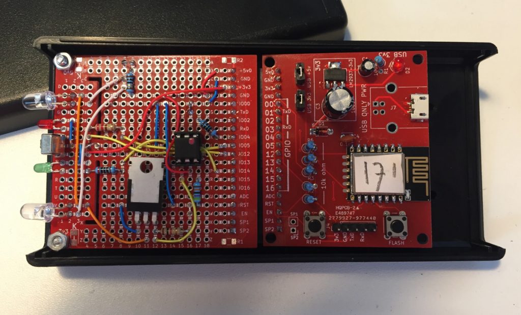
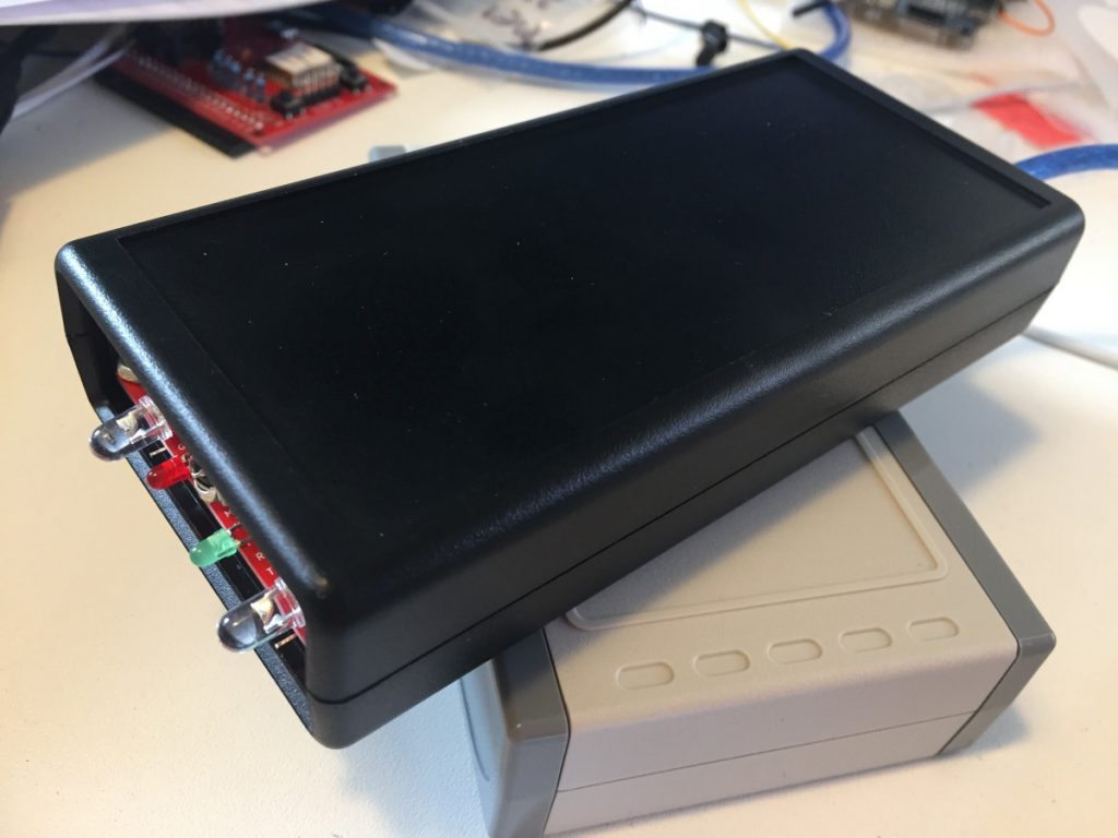
It makes a neat enclosure with the (IR) LED’s on one end and an USB power connector at the other end. Of course I have swapped the 1of!-Wemos board for a 1of!-ESP12.
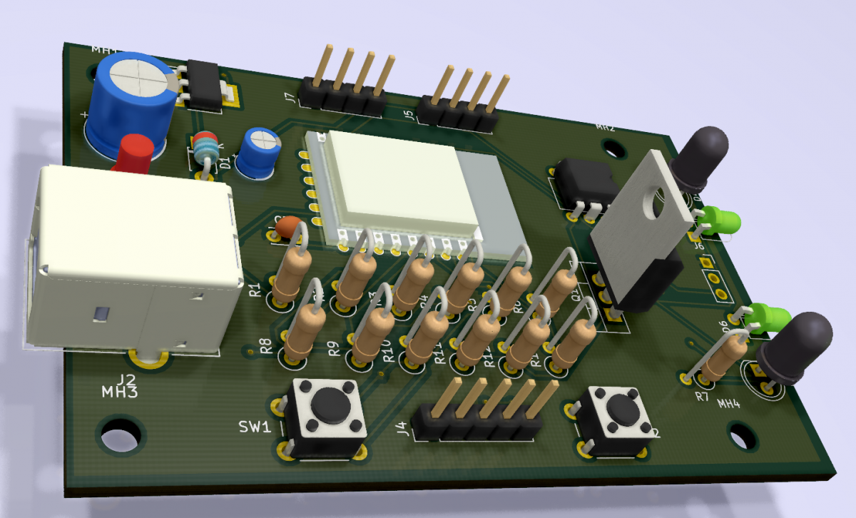
Making a Printed Circuit Board (PCB)
This is not a comprehensive guide on how to use KiCAD as there are tons of posts on the web and dozens of good books for that. I just want to show you the steps involved in the hope you will give it a try! Although KiCAD has a very steep learning curve, for me it is one of the best tools you can use for designing your own PCB’s.
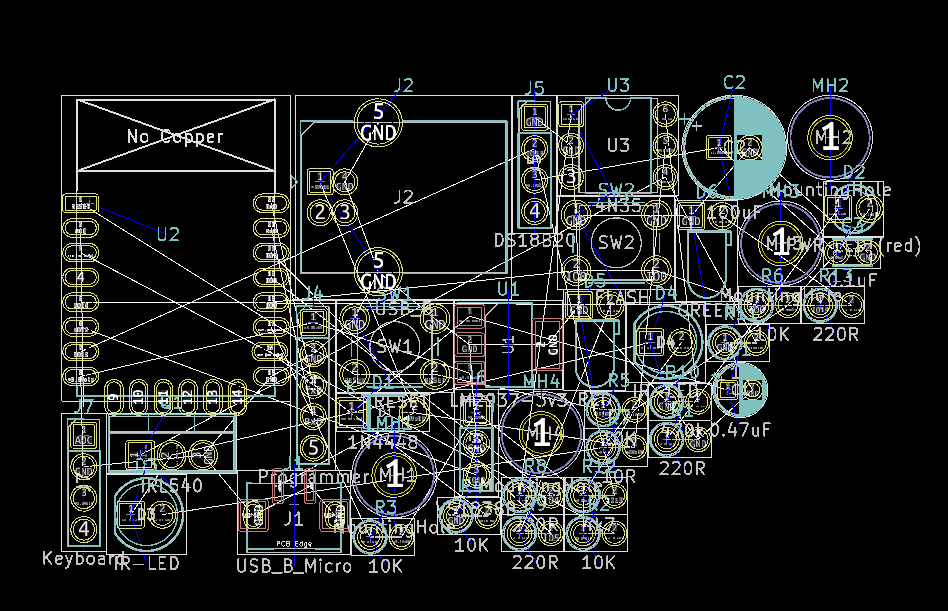
To be able to design a PCB for this device we need to combine the schematics of the 1of!-ESP12 processor board and the schematic of the IR-receiver and IR-sender.
In KiCAD you can import an existing schematic sheet into the schematic you are working on.
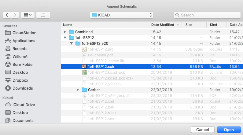
So, start with a new, empty sheet. In the File-menu select [Append Schematic Sheet]
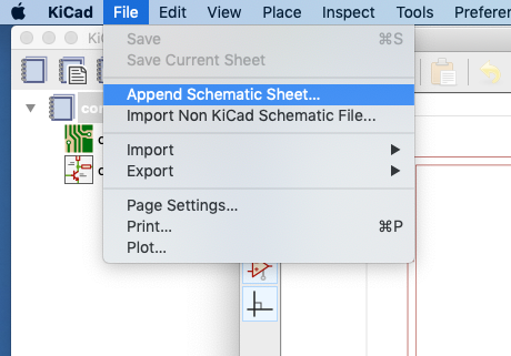
Then select the 1of!-ESP12.sch file (it’s in the map KiCad on the github repository).
Remove the 20-pin connector. Select the remaining objects and move them outside the sheet.
Now again select [Append Schematic Sheet] from the File-menu and select the Schematic for the IR-receiver and sender (you can find it in the map KiCad on the github repository).
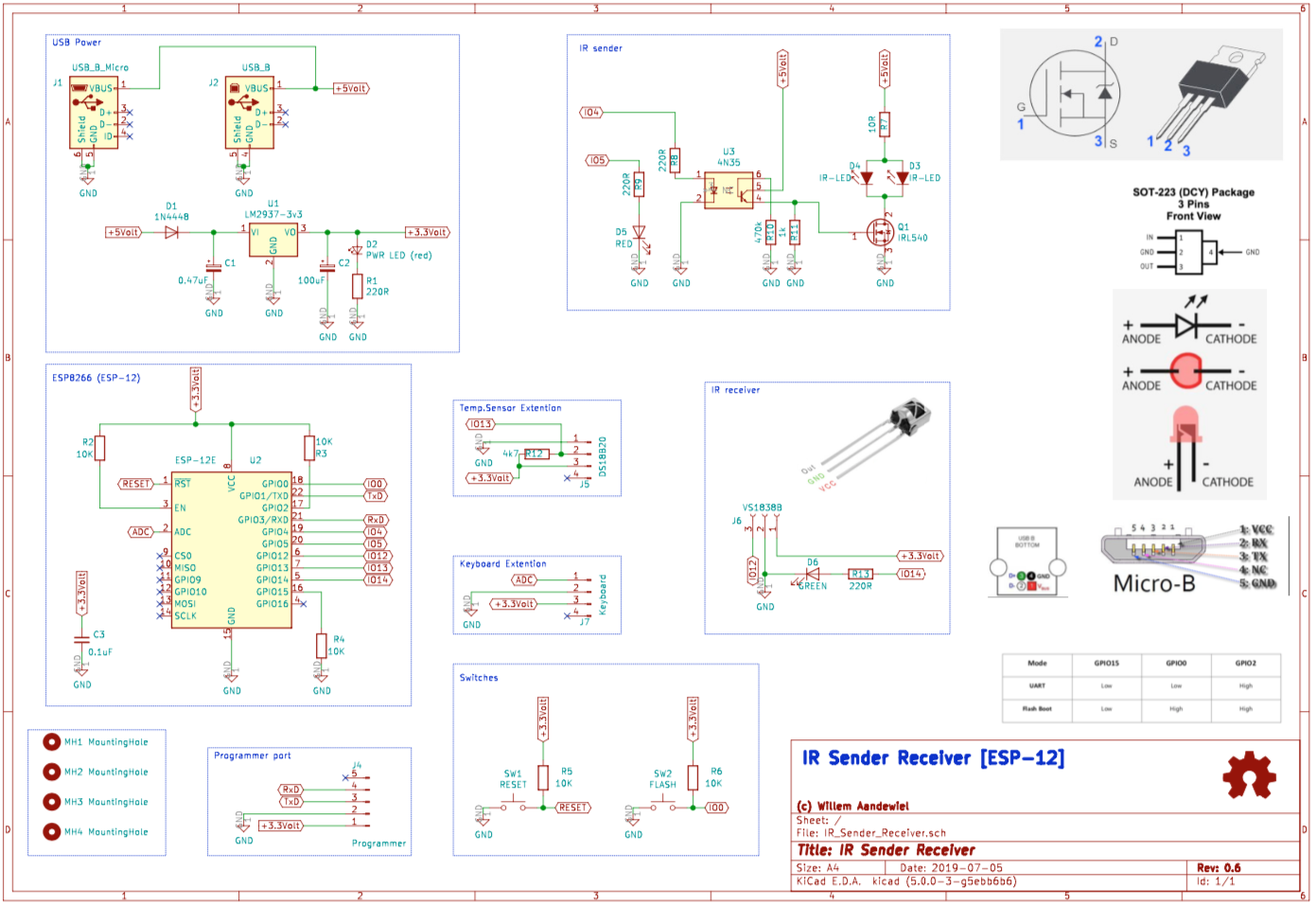
Remove the connector and move everything around till you have something like this:
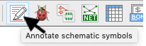
All field references have a question mark (?) so you need to press the annotate button.
After that all fields have a unique reference. Don’t worry, if your references are different from the ones in this post!
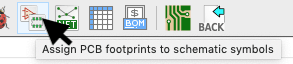
Next we need to associate physical parts to the parts in the schematic. This is done by assigning footprints to schematic symbols.
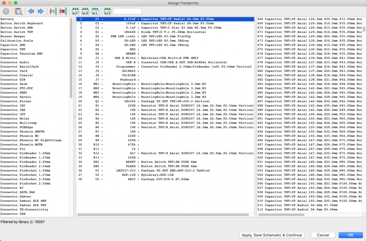
A new window pops-up. Most symbols are already assigned a footprint. For those that are empty you need to select the correct footprint from the right part of the window. On the left part of the window you can select specific groups of footprints. You can also create your own footprints with the footprint-editor and place them in a container of your own.
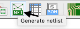
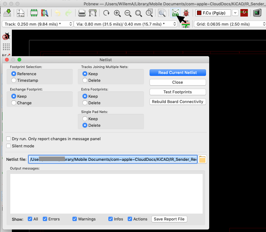
Next step is to generate a netlist. A netlist is the translation of the schematic to the PCB design.
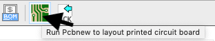
Press the PCBnew icon ..
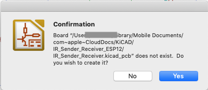
.. and a pop-up window will appear ..
.. asking if it’s OK to create a new PCB (this pop-up will only appear when there’s not already a PCB design).
Press [Yes] and an empty design window will open. In this window press the [Netlist] icon and select the [Read Current Netlist] to use the Netlist you created in the previous step and press [Close] to close this pop-up window.
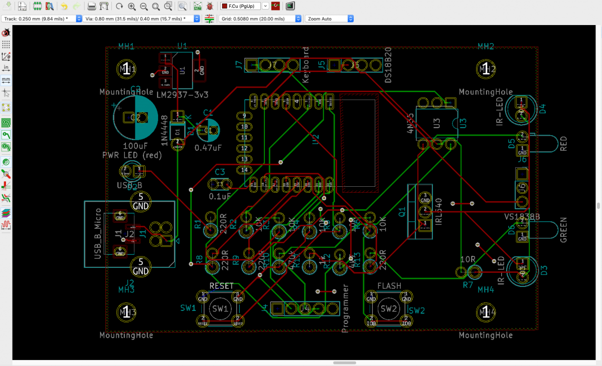
The big challenge is to move all the components to a logical place and connect them with copper traces till all the white lines in the rats nest are gone..
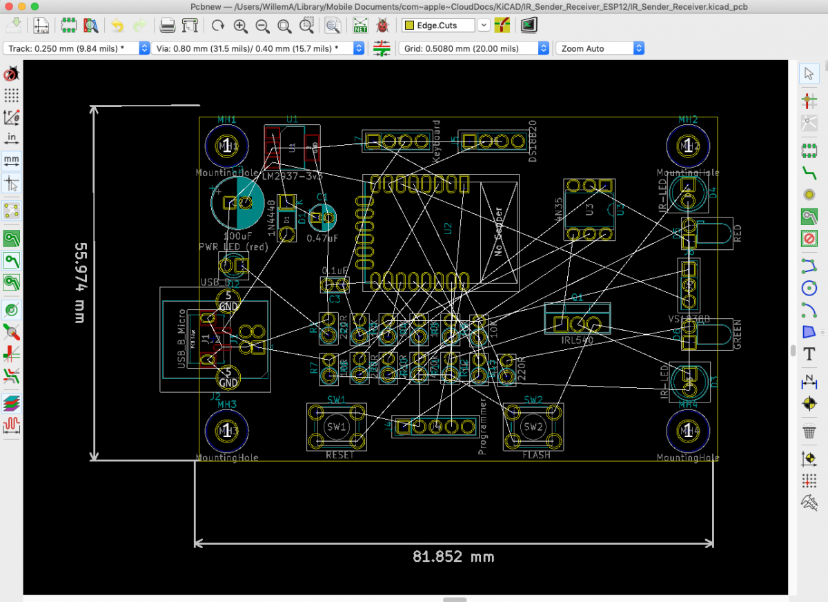
Time to lay the copper traces.
 Follow
Hoi Willem!
Leuk project, ik zocht nog zo iets! Ik wil mijn airco automatiseren op basis van sensoren van de omgeving (daarnaast ook de aansturing van een luchtbevochtiger en de automatische radiatorknoppen) om zo het klimaat op mijn kantoor optimaal te houden. Ik ga er zeker naar kijken!
Gr, Roland