[ 58,711 keer bekeken / views ]
Een Nederlandse vertaling van deze post kun je hier vinden.
With every electronic circuit I make, there comes a moment when the project is “finished”…. almost!
The last step is always to find a suitable projectbox and even then it is difficult to provide a (often plastic) projectbox with cutouts of the right size and in the right place.
Fortunately I have a 3D printer and in theory I can make a projectbox myself, but it always takes a lot of time. For standard processor boards you can find 3D STL files on the internet, but if you have “designed” a printed circuit board yourself, the only way is a “parameter controlled” solution that you can read in Fusion 360 or in openSCAD. Then you can specify the size of the box via parameters and sometimes a little more, but it never really “fits” well or it is so complex that you have to graduate before you can make something useful with it.
I think I’ve found a solution that can provide almost any printed circuit board with a nice projectbox: the YAPP generator!
In this post I explain what the principles of this YAPP generator are and how you can use it to 3D print beautiful projectboxes!
Dec. 4, 2023: Rev 3.0 released
This release breaks with almost all API’s!
Here you can find the official documentation.
What you need
- openSCAD
A recent version of “openSCAD” can be downloaded here. - the YAPP generator
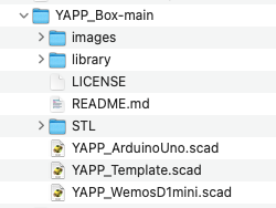
You can download this as a “.zip” file from github. Extract the “YAPP_Box-main.zip” file into your openSCAD projects folder. You now have a new folder “YAPP_Box-main” containing several sample files. In “YAPP_Box-main” there is also a folder “library” that contains the YAPP generator (so don’t throw it away!). It is wise to leave the folder structure as it is and save new box designs in this “YAPP_Box-main” folder.
Design philosophy
Most box generators that you can find on the internet allow you to specify the size of the box. Sometimes you have to give inside measurements and sometimes outside measurements.
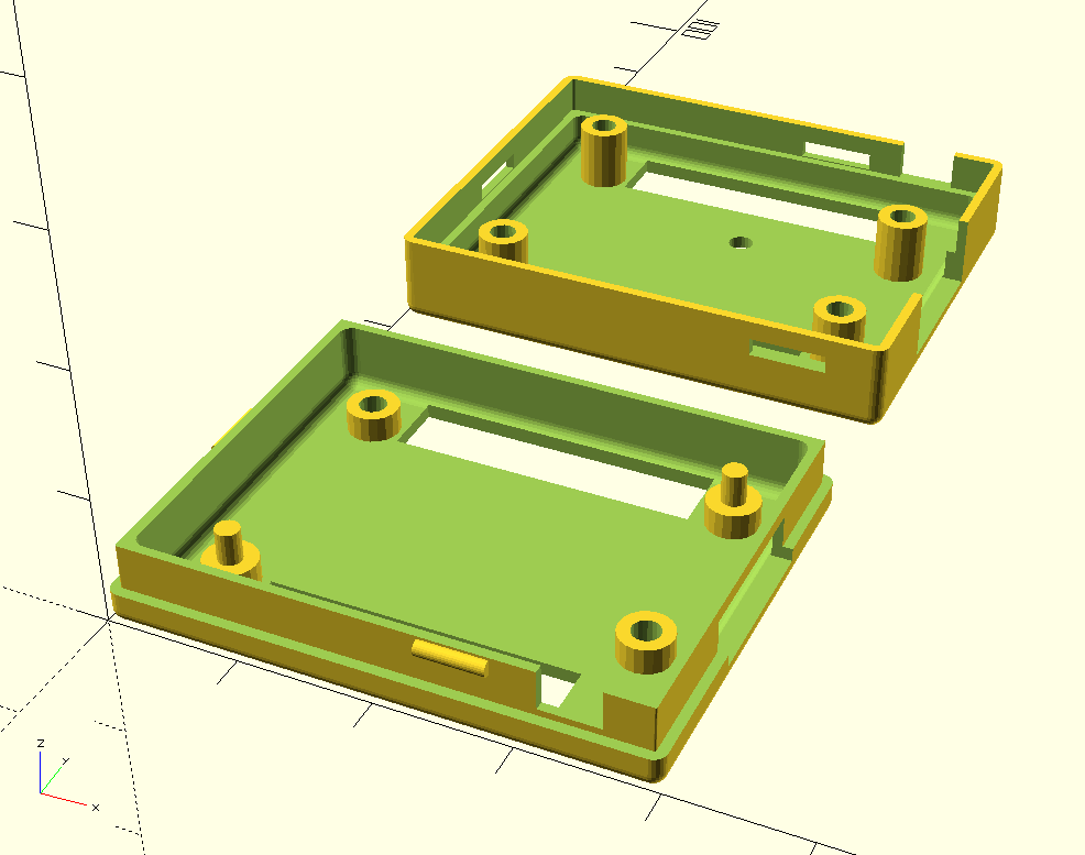
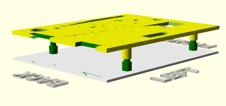
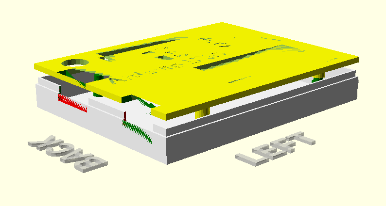
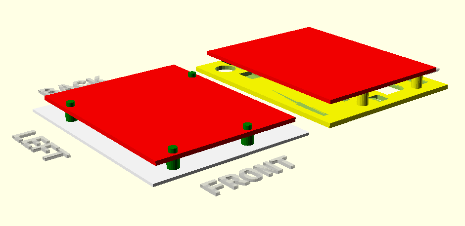
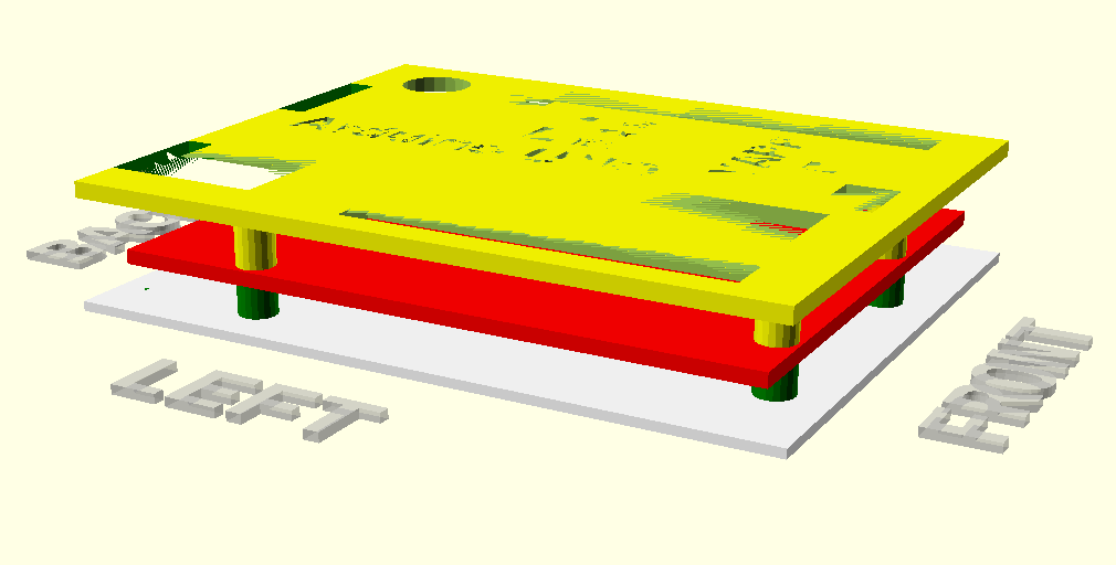
YAPP does this differently and starts from the printed circuit board for which you need a projectbox. The most important measurements are therefore the length, width and thickness of the printed circuit board. Then you specify where the holes are with which the printed circuit board should be secured. The holes can be used to secure the PCB with screws or you can clamp the PCB between the standoffs in the bottom and top of the projectbox. Then you can specify for all surfaces (lid, base, front, back, left and right) of the projectbox where rectangular and/or round cutouts should be placed.
Finally, texts can be entered that will be printed at the lid of the projectbox.

basis you can make complex project boxes
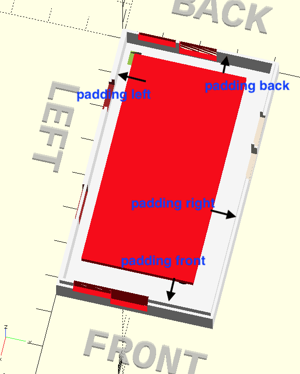
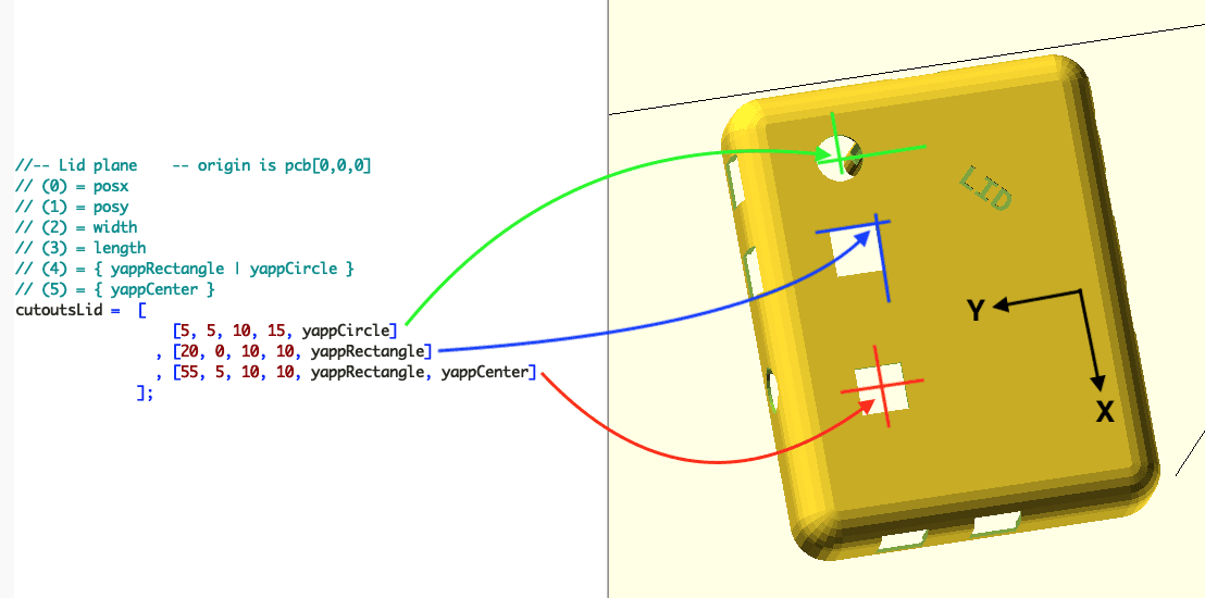
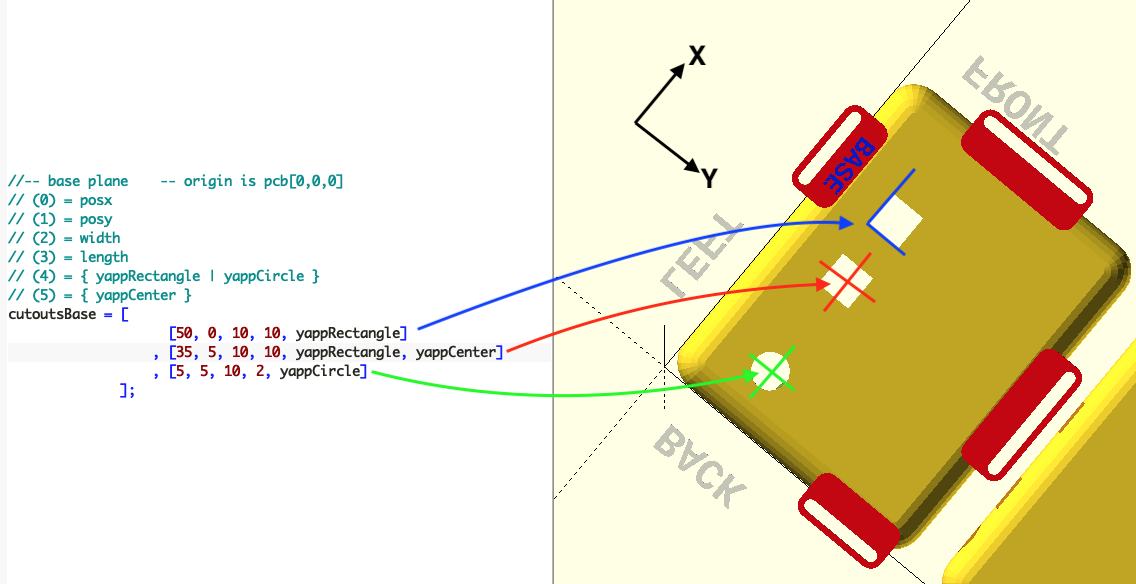
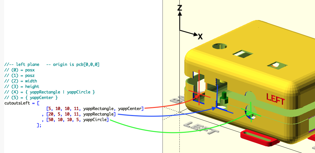
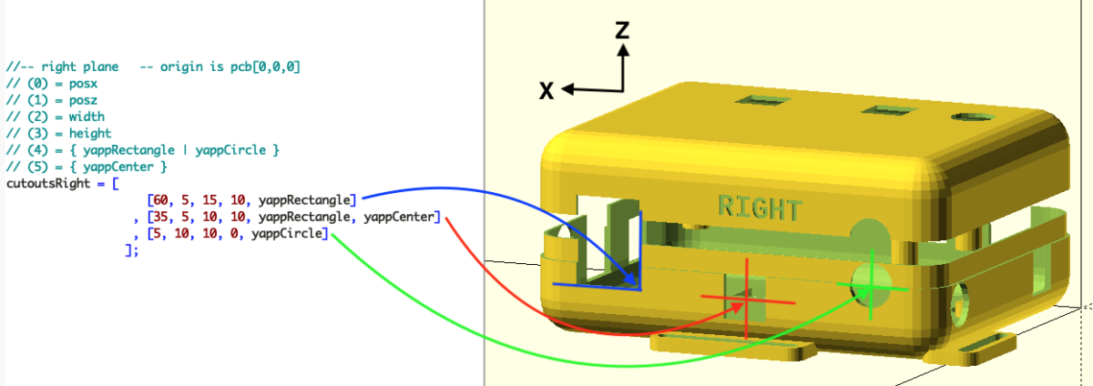
Coördination System
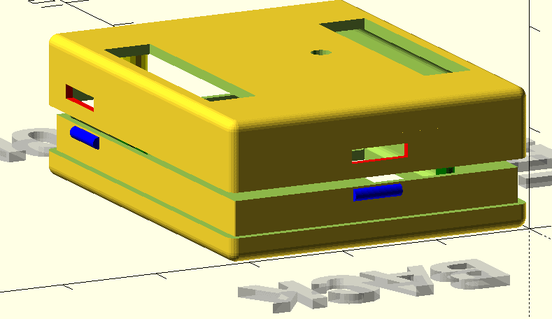
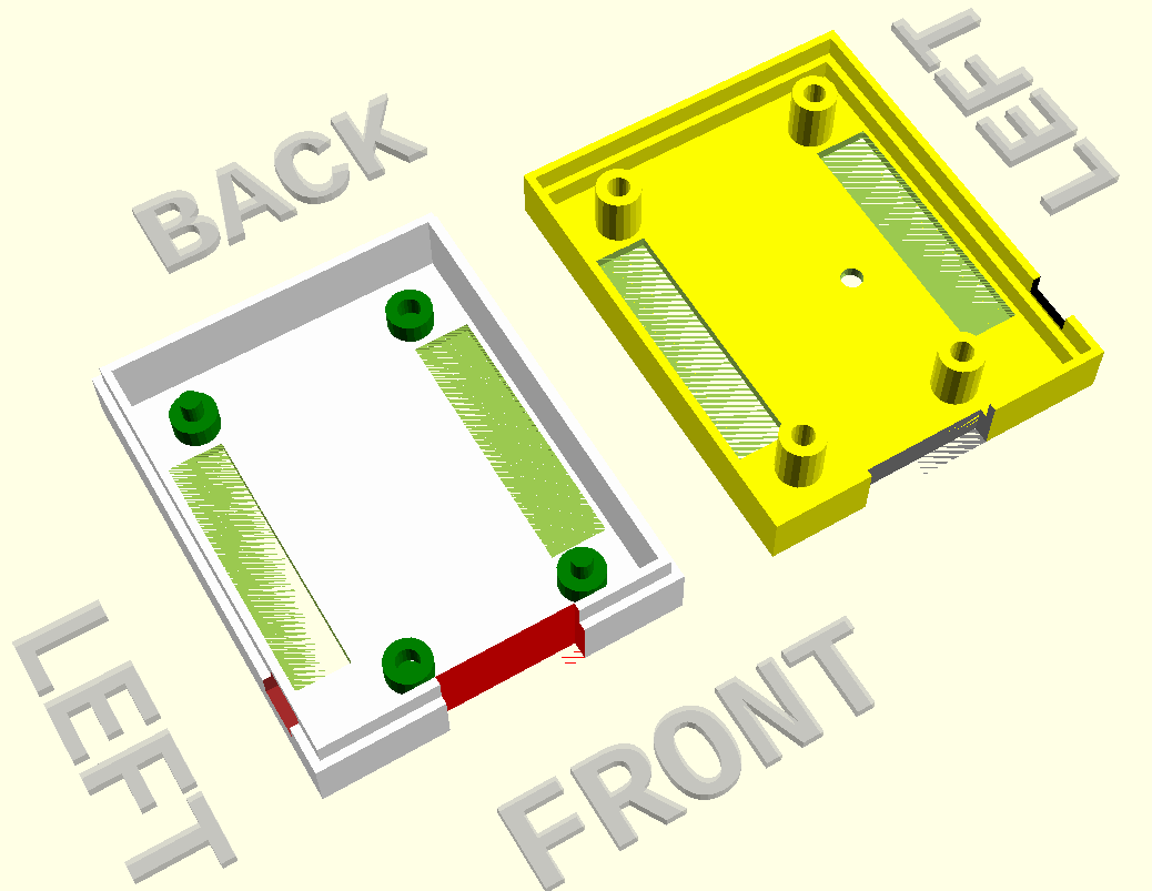
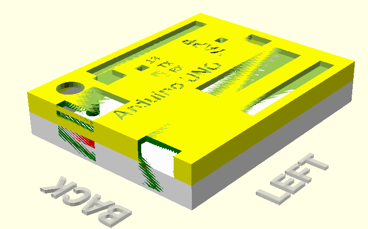
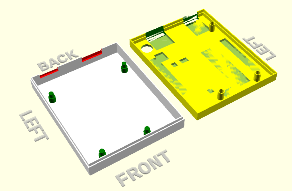
Before going further it is necessary to understand what the orientation of the projectbox is. It should be clear that the projectbox has six “planes”.
The top is called “lid” the bottom is called “base”. The plane closest to the Y-axis is the “back”. “left” is closest to the X-axis. The plane opposite “back” (which is furthest from the Y-axis) is called “front” and the plane opposite “left” is called “right”
The “zero point” ([x=0, y=0, z=0]) is always left-back at the top of the PCB.
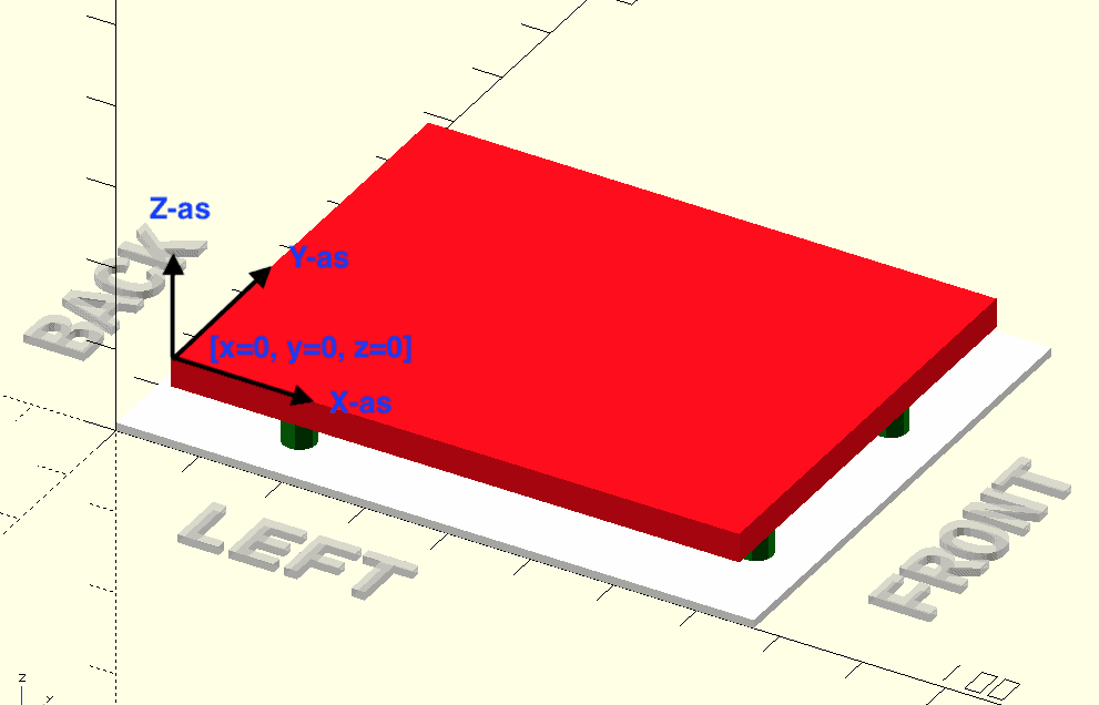
For each plane there is an array in which you can specify where the cutouts should be in that plane. These cutouts all have (pcb)[0,0,0] as their starting point. So if at any time it is decided to enlarge the edges around the PCB (padding) or to make the “pcbStandoffs” higher, the cutouts will move neatly with the position of the PCB.
Cutouts
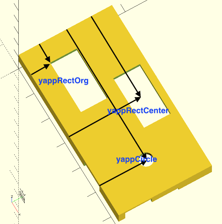
There are two types of cutouts: “rectangles” and “circles”. Rectangles can be created in two ways, either with the corners at coordinates or with coordinates in the center of the rectangle. For “circles” the coordinates are always the center point.
Standoffs
The “pcbStandoffs” defines the distance between the top of the “base plane” and the bottom of the printed circuit board. Opposite the “standoffs” are automatically made “pushdowns” on the “lid” that are exactly so long that the circuit board is neatly clamped between them.
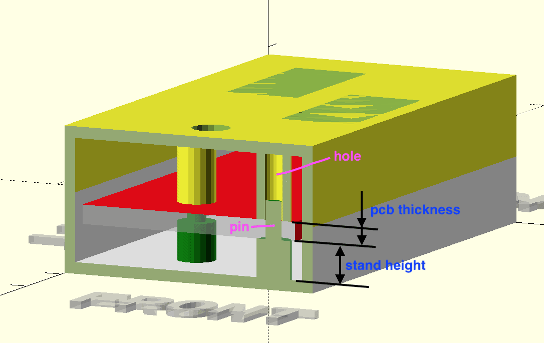
The standoffs can be fitted with “pins” so that the printed circuit board is also fixed on the X and Y axes. How many “pcb standoffs” should come and where they should be is specified in the array “pcbStands”. Each pcbStand is specified in one line and the properties of a pcbStand are defined per line.
This is how you use the pcbStands arrayt:

Each line in the array provides one standoff.
The third (2) element has the following meaning:
 yappBoth:       place both below a pcbStand and above a pcbStand.
 yappLidOnly:    the pcbStand is only printed above (lidHalf)
 yappBaseOnly:   the pcbStand will only be printed at the base (baseHalf).
The meaning of the fourth (3) element is:
 yappHole:    the pcbStand is provided with a “hole” (hole)
 yappPin:     the pcbStand is provided with a “pin”
If the third (2) element is “yappBoth” and the fourth (3) element is specified as “yappPin” then the pin will be printed on the baseHalf and a hole on the lidHalf.
It is possible to print both below and above a hole by specifying “yappHole” as the fourth (3) element:
[3, 12, yappBoth, yappHole]
If you like this post please consider a small donation
Cutouts in the six faces
Pay attention!
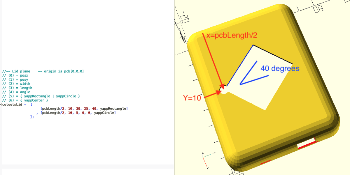
All examples are made with version 1.3 of the YAPPgenerator. From version 1.4 on the rows in the cutouts arrays have an extra parameter “angle”. For existing designs it suffices to add them with the value “0” (zero) directly before yappRectangle or yappCircle.
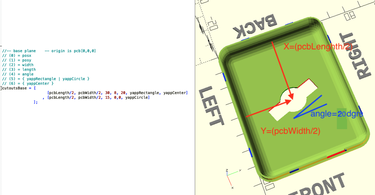
For each face there is an array in which you can specify per line where cutouts should come, what the origin of such a recess is (for rectangles) and what shape the recess should have (rectangle or circle). Depending on the “plane”, the first element is the position on the X-axis (lid-, base-, left- or rightPlane) or the Y-axis (front- or backPlane) and the second element is the position on the Y-axis (lid-, base-, left- or rightPlane) and the Z-axis (front-, back-, left- or rightPlane). The third element always indicates the width of the rectangle or the diameter of the circle. The fourth element is, again depending on the plane, the width (lid- or basePlane) or the height (front-, back-, left- or rightPlane) of the rectangle.
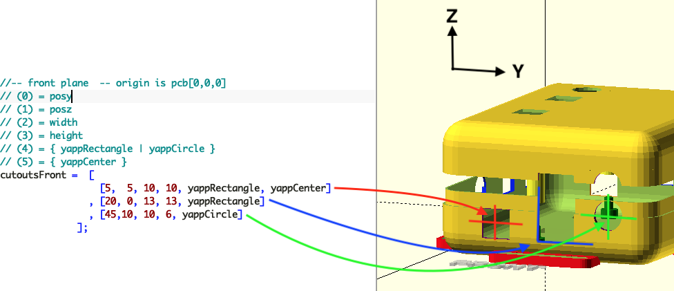
Cutouts in the Front Plane
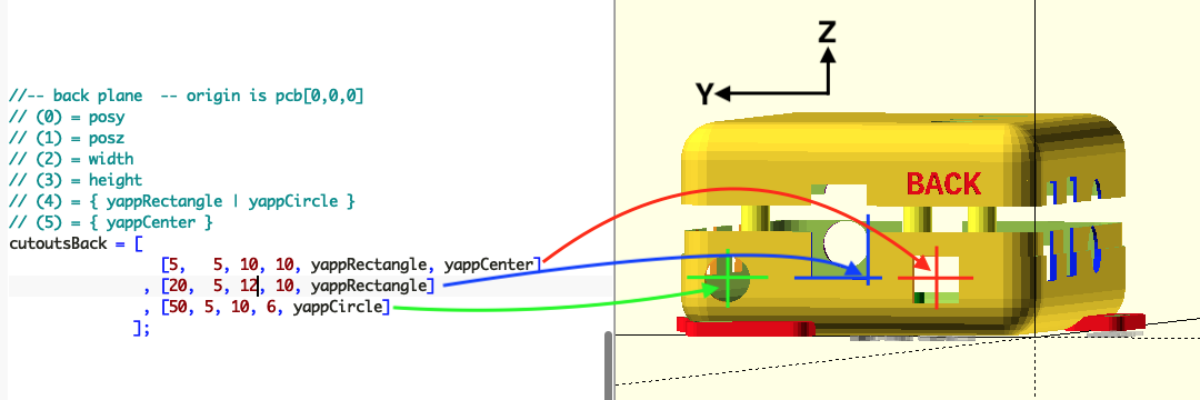
Cutouts in the Back Plane
Cutouts in the Lid Plane
Cutouts in the Base Plane
Cutouts in the Left Plane
Cutouts in the Right Plane
Rectangular cutout at an angle
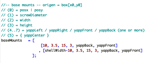
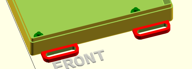
Base Mounts
To be able to mount the project box you can define so called “Base Mounts”.
Connectors to connect Base and Lid together
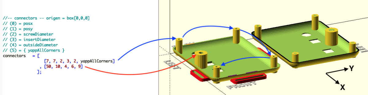
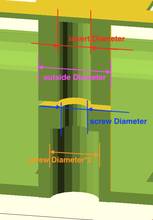
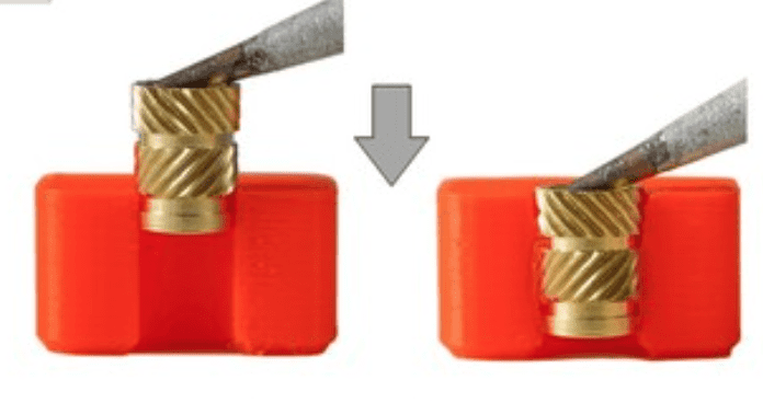
The connectors are ideal for connecting the two halves with so-called “inserts”.
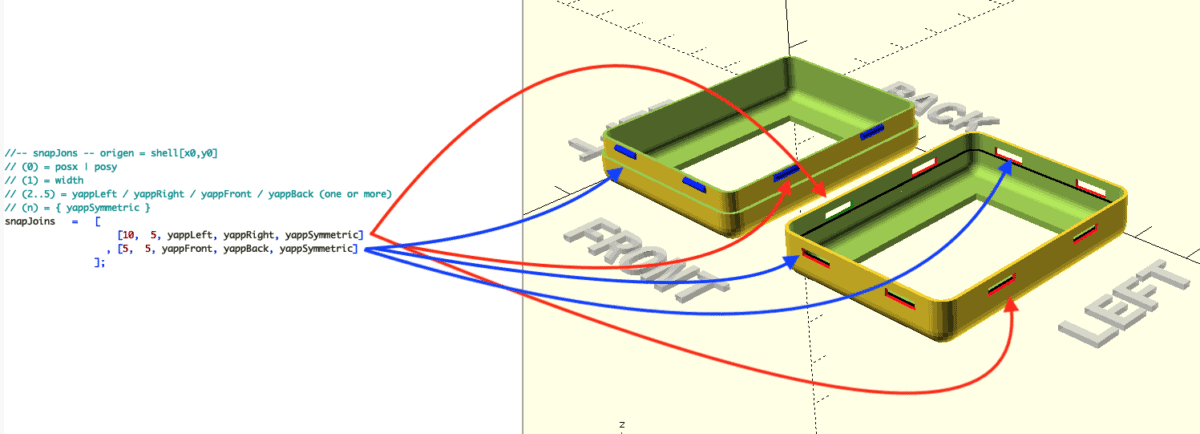
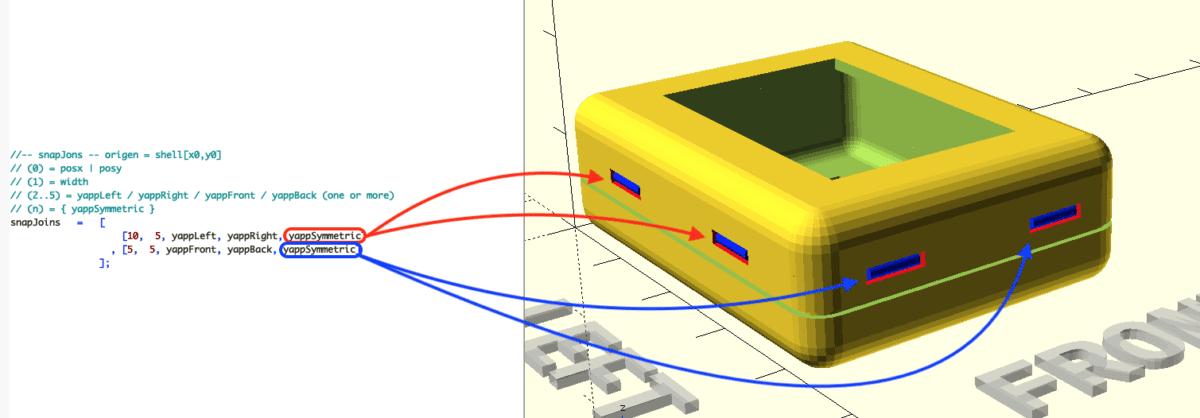
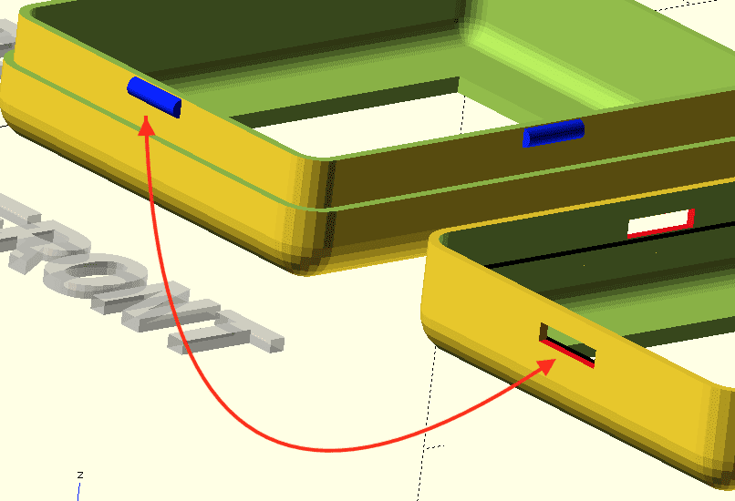
Snap Joins
With snapJoins the Base and Lid “click” together without the need for screws or other aids.
If you like this post please consider a small donation
A life real example
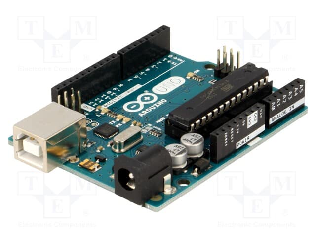
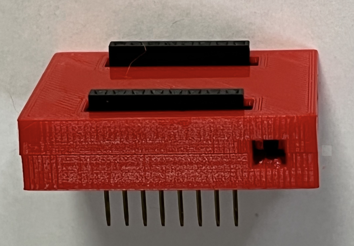
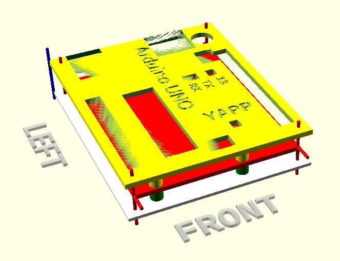
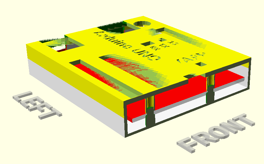
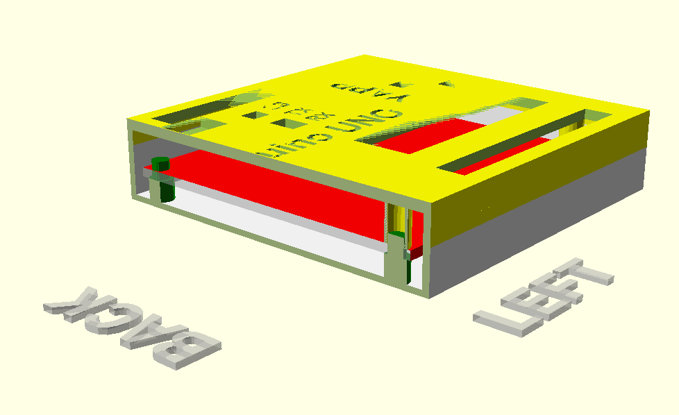
In this example we are going to create a projectbox for an Arduino UNO.
We start in openSCAD by opening the file “YACC_template.scad” and immediately save it again (“[Save as]) with the name “ArduinoUNO”.
Make sure that the new file is saved in the folder “YAPP_Box-main”.
Now edit the comment lines at the top of the file so that it is clear that a projectbox for an Arduino UNO can be generated with this file. The first real line of code inserts the YACC generator after which the YAPPgenerate() module from this library can be used.
include <./library/YAPPgenerator_v13.scad>
Outer dimensions and stand-offs
Now all variables that determine the final projectbox must be measured one by one and entered into the “ArduinoUNO.scad” file.
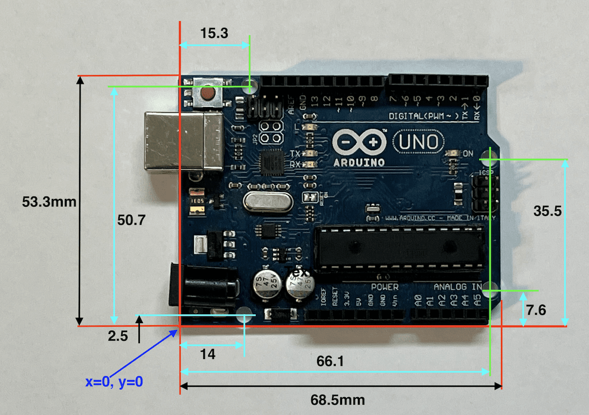
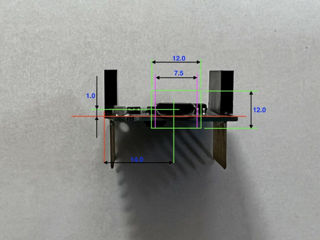
pcbLength    = 68.5;
pcbWidth     = 53.3;
pcbThickness = 1.5;

pcbStands = [
                 [14.0, 2.5,  yappBoth,     yappPin]  // back-left
               , [15.3, 50.7, yappBaseOnly, yappPin]  // back-right
               , [66.1, 7.6,  yappBoth,     yappPin]  // front-left
               , [66.1, 35.5, yappBoth,     yappPin]  // front-right
            ];
Connectors
The height of both the USB plug and the powerJack is 11mm.
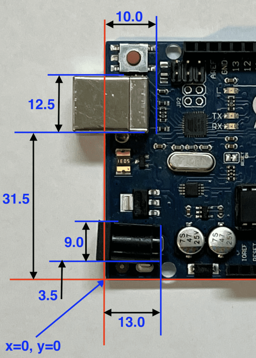
To add some slack, let’s start the USB plug and the powerJack 1mm closer to the X-axis and increase the width of the cutout for the USB plug by 2mm and the cutout for the powerJack by 3mm. We will also increase the length of both cutouts slightly.
cutoutsLid = [
                 [0, 31.5-1, 12.2+2, 11.0, yappRectOrg] // USB
               , [0, 3.5-1,  12.0,   13.5, yappRectOrg] // Power Jack
             ];

cutoutsBack = [
                 [31.5-1, -1, 12.2+2, 12, yappRectOrg] // USB
               , [ 3.5-1,  0, 12.0,   11, yappRectOrg] // Power Jack
             ];
Headers and ATmega
cutoutsLid = [
                [0, 31.5-1, 12.2+2, 11.0,           yappRectOrg] // USB
              , [0, 3.5-1,  12.0,   13.5,           yappRectOrg] // Power Jack
              , [29-1,      12.5-1,  8.5+2, 35.0+2, yappRectOrg] // ATmega328
              , [17.2-1,    49.5-1,  5.0, 47.4+2,   yappRectOrg] // right headers
              , [26.5-1,     1.0-1,  5.0, 38.0+2,   yappRectOrg] // left headers
             ];
Other cutouts
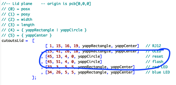
Finally, the positions and size of the ICSP connectors, reset button and LEDs must be measured.
The total definition of the cutoutsLid array then looks like this:
cutoutsLid =  [
                 [0,      31.5-1, 12.2+2, 11.0,   yappRectOrg]    // USB
               , [0,       3.5-1, 12.0,   13.5,   yappRectOrg]    // Power Jack
               , [29.0-1, 12.5-1, 8.5+2,  35+2,   yappRectOrg]    // ATmega328
               , [17.2-1, 49.5-1, 5.0,    47.4+2, yappRectOrg]    // right headers
               , [26.5-1,  1.0-1, 5.0,    38.0+2, yappRectOrg]    // left headers
               , [65.5,   28.5,   8.0,     5.5,   yappRectCenter] // ICSP1
               , [18.0,   45.5,   6.5,     8.0,   yappRectCenter] // ICSP2
               , [6.0,    49.0,   8.0,     0.0,   yappCircle]     // reset button
//-- if space between pcb and lidPlane > 5.5 we don't need holes for the elco's --
//             , [18.0,    8.6,   7.2,     0.0,   yappCircle]     // elco1
//             , [26.0,    8.6,   7.2,     0.0,   yappCircle]     // elco2
//             , [21.5,    8.6,   7.2,     7.0,   yappRectCenter] // connect elco's
               , [28.2,   35.2,   5.0,     3.5,   yappRectCenter] // TX/RX leds
               , [28.2,   42.5,   3.0,     3.5,   yappRectCenter] // led13
               , [58.5,   37.0,   3.0,     3.5,   yappRectCenter] // ON led
              ];
In order to actually generate the projectbox, this module call must be placed at the bottom of the program:
     //--- this is where the magic happens ---
     YAPPgenerate();
Then click on [F5] or [F6] to see the result of your work.
Second example (Wemos D1)
In this example we will create a projectbox for a Wemos D1 mini (V3.0.0). The starting point is again the YAPP_template.scad file which we read in and immediately write back as “WemosD1Mini.scad“.
First we have to measure all sizes again.
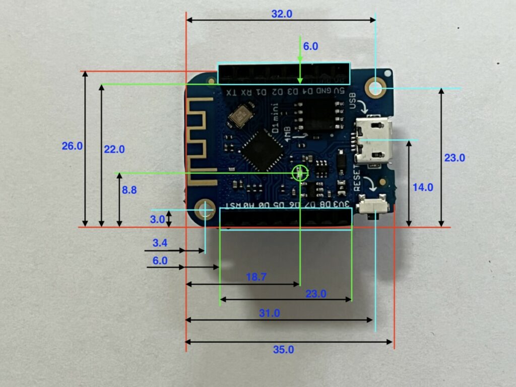
The “outer dimensions” are put at the top of the script.
 wallThickness        = 1.5;
 basePlaneThickness   = 1.0;
 lidPlaneThickness    = 1.0;

 baseWallHeight       = 4;
 lidWallHeight        = 4;

 pcbLength            = 35.0;
 pcbWidth             = 26.0;
 pcbThickness         = 1.0;

 // padding between pcb and inside wall
 paddingFront         = 1;
 paddingBack          = 1;
 paddingRight         = 1.5;
 paddingLeft          = 1.5;

 // ridge where base and lid off box can overlap
 // Make sure this isn't less than lidWallHeight
 ridgeHeight          = 2;
 ridgeSlack           = 0.1;

 // How much the PCB needs to be raised from the bottom
 // to leave room for solderings and whatnot
 standoffHeight       = 2.0;
 pinDiameter          = 1.8;
 pinHoleSlack         = 0.1; // depending on nozzle diameter
 standoffDiameter     = 4;
The positions and size of the cutouts are included in the cutoutsLid, cutoutsBase, cutoutsFront, and cutoutsRight arrays.
//-- pcb standoffs -- origin is pcb-0,0
pcbStands =    [
                   [3.4,         3.0,        yappBoth, yappPin]  // back-left
                 , [3.4,         pcbWidth-3, yappBoth, yappHole] // back-right
                 , [pcbLength-3, 7.5,        yappBoth, yappHole] // front-left
                 , [pcbLength-3, pcbWidth-3, yappBoth, yappPin]  // front-right
               ];

//-- front plane -- origin is pcb-0,0 (red)
cutoutsFront = [
                    [14.0, 1.0, 12.0, 10.0, yappRectCenter] // microUSB
               ];

//-- top plane -- origin is pcb-0,0
cutoutsLid =   [
                    [6.0, -1.0,       6.0, pcbLength-12, yappRectOrg] // left-header
                  , [6.0, pcbWidth-4, 6.0, pcbLength-12, yappRectOrg] // right-header
                  , [18.7, 8.8,       2.0, 0.0,          yappCircle]  // blue led
               ];

//-- bottom plane -- origin is pcb-0,0
cutoutsBase =  [
                    [6.0, -1.0,       6.0, pcbLength-12, yappRectOrg] // left-header
                  , [6.0, pcbWidth-4, 6.0, pcbLength-12, yappRectOrg] // right-header
               ];

//-- left plane -- origin is pcb-0,0
cutoutsLeft =  [
                    [31.0, 0.5, 4.5, 3, yappRectCenter] // reset button
               ];
Note that there are only two holes in the circuit board. To keep the printed circuit board in place, four pcbStand are made, but two of them have no pins. Because there is a reset switch in the left front corner, the pcbStand must also be placed in a slightly shifted place in this corner.
Last step is to make some “snapJoins” in the left, right and front panes:
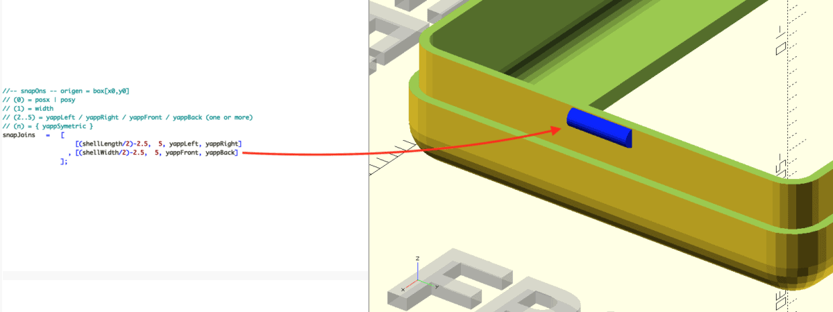
//-- snap Joins -- origen = box[x0,y0]
// (0) = posx | posy
// (1) = width
// (2..5) = yappLeft / yappRight / yappFront / yappBack (one or more)
// (n) = { yappSymmetric }
snapJoins   =   [
                    [shellLength-17, 5, yappLeft]
                  , [shellLength-10, 5, yappRight]
                  , [(shellWidth/2)-2.5, 5, yappBack]
                ];
Finally, the YAPPgenerate() module must be called:
   //--- this is where the magic happens ---
   YAPPgenerate();
Then press [F5] or [F6] to check if the project box looks as you imagined.
Debug options
There are several options for viewing additional information about the generated projectbox so that it can be checked during the design phase whether the script does what it should do.
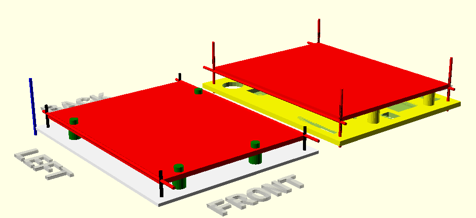
  printLidShell    = true;
  printBaseShell   = true;

  //-- D E B U G -------------------- default
  showSideBySide      = true;      // true
  hideLidShell        = false;     // false
  colorLid            = "yellow";  // yellow
  hideBaseShell       = false;     // false
  colorBase           = "white";   // white
  showPCB             = false;     // false
  showPCBmarkers      = false;     // false
  inspectX            = 0;         // 0=none, -pcbLength .. +pcbLength
  inspectY            = 0;         // 0=none, -pcbWidth .. +pcbWidth
  //-- D E B U G -------------------
The first two variables (printLid and printBase) indicate whether the top half of the projectbox or the bottom half should be printed. This can be useful if your 3D printer is not large enough to print both halves side by side or if you have only made adjustments in one of the two and (so) only want to 3D print that half again.
showSideBySide
hideLidShell / hideBaseShell
This setting provides insight into the “inside” of the projectbox.
showPCB
This option is especially useful in side-by-side presentation or when showLid and/or showBase are “false”.
showPCBmarkers
Markers are displayed on the four corners of the circuit board and on the rear left corner of the box.
inspectX / inspectY
With a value of -pcbLength to +pcbLength, a cross section of the projectbox is shown.
Other Exampels
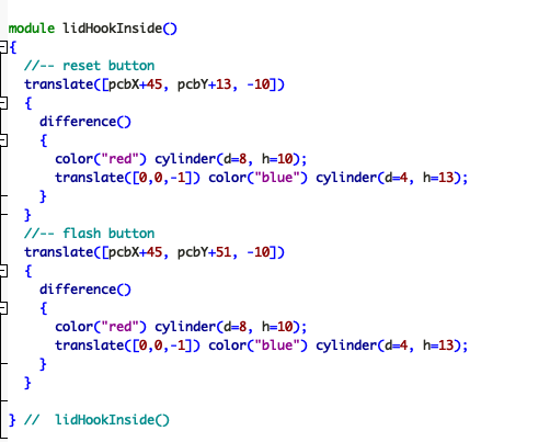
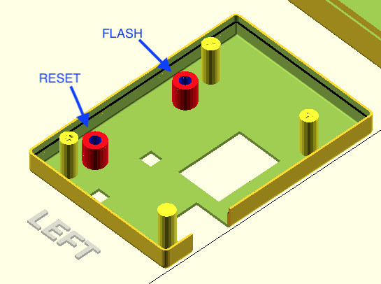
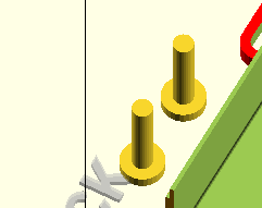
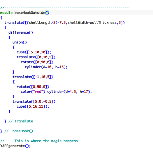
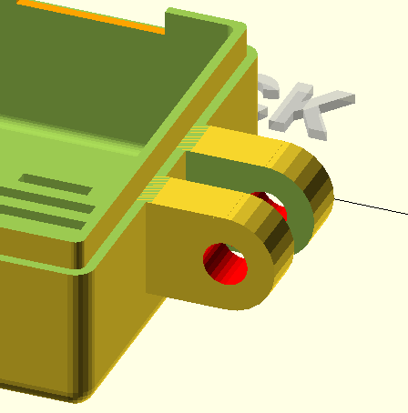
In special cases you want to be able to create objects that cannot be created with the standard arrays. For this, there are four so-called “hooks” that make it possible to define these special objects in the project box or outside the project box. These hooks are called:
- lidHookInside()
- baseHookInside()
- lidHookOutside()
- baseHookOutside()
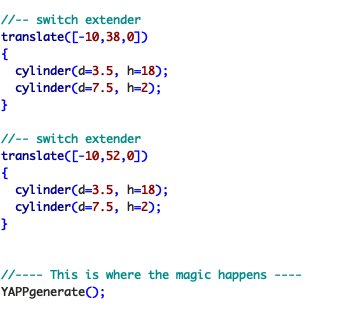
Suppose you have two push buttons on the PCB that you of course want to be able to operate when the PCB is in the project box. Three things have to be arranged for this.
- You have to define two round holes in the Lid;
- On the inside of the lid there should be two round guides for the “switchExtenders”;
- The switchExtenders must be printed. Because they are not connected to the project box, they can be included in a separate scad file or simply printed “next to the project box”.
For an ESP-CAM you want to make it possible to put it “tiltable” on a foot. You can use the “lid- or baseHookOutside” modules for this.
Snap Joins
A “snapJoin” is a bulge in the Base that fits exactly in a hole in the Lid. A snapJoin clicks the Lid onto the Base without screws or anything else.
Often you want the snapJoins to be applied symmetrically on one or two sides. This can be done by specifying “yappSymmetric” in a snapJoin row as the last argument.
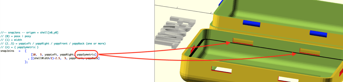
Note: snapJoins can only be created if the ridgeHeight is not lower than 3mm!
 Follow
The above “Arduino Uno” example no longer compiles when using YAPPgenerator_v3.scad – I get these error messages:
Ignoring unknown variable ‘yappRectOrg’
Ignoring unknown variable ‘yappRectCenter’
Luckily there is a working example in the GitHub repo:
Cause of the issues is the cutout type definition names having changed between versions.
Great project!
How about preventing cutouts that don’t extends through the edge of lid or base.
They can block the insertion of the circuit board, when having them on opposite sides (USB) .
Hi Gunner,
It is probably best if you add an issue on github.
Regards
… come to think of it, you can just use the inside and outside hooks to remove the (parts) around the normal cutout (for the USB) you don’t want. It is a bit fidling to position the hooks but it does exactly what you need.
Or …
Just make the cutout bigger!
I don’t understand how a hook can “subtract” things.
But I did this:
difference()
{
YAPPgenerate();
translate([ 0 ,15.125 + wallThickness + paddingLeft, myPcbZ + 1.6])
cube([5,7.800, baseWallHeight]);
}
For showSideBySide = true:
It’ works fine. (Ok for generating 3D-print)
else:
It also wrongly cuts in the lid. (Looking ugly)
Hello, This is a great library. I played with it and created a box for my latest project. One issue I have is that my lid design (the box cover) needs to be not flat but have two different heights as I have a display that is lower in height compared with some other components and I want the lid to be close to it. Is there a way to design the lid to have a few heights? Thanks a lot!
Hi Motti,
No, that is not possible.
But what you cán do is use hooks to accomplish what you want. Please post an image of the end result!
Hi Willem, Thanks for your reply! I have seen some text about the hooks but did not fully understand this. Is it possible for you to point me to relevant examples on how to use that and/or some more explanations? Thanks a lot!
I do not have an example for your specific use case but with a hook you can extend the box with almost everything you want (or need).
Here you find a simple example.
And, of course you need to read the documentation!
You will need to fiddle a bit to get things working the way you want it to be but sure, it can be done!
Hi Willem,
I looked at the hooks documentation and example. It does not say a lot. As I need to have the lid in some of its areas in a different height, I need to cut out parts of the lid and build other levels by myself. I can I do a difference() on the current design so that the required pieces are cut out, and how can I add the new heights (with their walls)? I can’t figure this out and will appreciate your help on that. Thanks a lot!
Motti,
From the top of my had.
First create a cutout in the lid the size you need an elevated level for.
Then: with an outside hook create a box of the size of the cutout and then hollow the box.
Something like:
difference()

{

    cube([…]); // outside

    cube([…]); // inside - hollow

}
And with translate([…]) position the box over the cutout
Hi Willem, version 1 of my box 🙂
I used the hooks mechanism to make this.
Requires more work but moving forward.
I am using a Prusa Mini. Its support structure (I needed that) is not good as you can see this ugly surface below the buttons.
Moving on…
Thanks a lot!
Hi Motti,
Great job.
Although I don’t quite understand why you need different levels on the lid.
You could do this with inside hooks and just position walls around the display ..?
If you do that you can also use the push-button function.
Look here for the openScad files.
Is there an example available where it is explained how to add two different printed circuits in a box, side by side, with different height and stand-offs? I have done all the measurements but struggle with the code.
Many thanks in advance for your help, thanks for this great tool!
I was, as we speak, working on a box with two PCB’s in it:
//-----------------------------------------------------------------------

// Yet Another Parameterized Projectbox generator

//

//  This is a box for openTherm Master / Slave boards

//

//  Version 3.3.0 (2024-11-27)

//

//-----------------------------------------------------------------------
include <./YAPPgenerator_v3.scad>
//-- which part(s) do you want to print?
printBaseShell = true;
printLidShell = true;
printSwitchExtenders = true;
printDisplayClips = true;
// ********************************************************************
// The Following will be used as the first element in the pbc array
//Defined here so you can define the "Main" PCB using these if wanted
pcbLength = 35; // front to back (X axis)
pcbWidth = 26; // side to side (Y axis)
pcbThickness = 16;
standoffHeight = 2.0; //-- How much the PCB needs to be raised from the base to leave room for solderings and whatnot
standoffDiameter = 7;
standoffPinDiameter = 2.4;
standoffHoleSlack = 0.4;
//===================================================================
// *** PCBs ***
// Printed Circuit Boards
//-------------------------------------------------------------------
// Default origin = yappCoordPCB : yappCoordBoxInside[0,0,0]
//
// Parameters:
// Required:
// p(0) = name
// p(1) = length
// p(2) = width
// p(3) = posx
// p(4) = posy
// p(5) = Thickness
// p(6) = standoff_Height
// p(7) = standoff_Diameter
// p(8) = standoff_PinDiameter
// Optional:
// p(9) = standoff_HoleSlack (default to 0.4)
//The following can be used to get PCB values elsewhere in the script - not in pcb definition.
//If "PCB Name" is omitted then "Main" is used
// pcbLength --> pcbLength("PCB Name")
// pcbWidth --> pcbWidth("PCB Name")
// pcbThickness --> pcbThickness("PCB Name")
// standoffHeight --> standoffHeight("PCB Name")
// standoffDiameter --> standoffDiameter("PCB Name")
// standoffPinDiameter --> standoffPinDiameter("PCB Name")
// standoffHoleSlack --> standoffHoleSlack("PCB Name")
pcb =
[
// Default Main PCB - DO NOT REMOVE the "Main" line.
["Main", pcbWidth, pcbLength, 0,0, pcbThickness, standoffHeight, standoffDiameter, standoffPinDiameter, standoffHoleSlack]
, ["Second", pcbWidth, pcbLength, 40,0, pcbThickness, standoffHeight, standoffDiameter, standoffPinDiameter, standoffHoleSlack]
];
//-------------------------------------------------------------------
//-- padding between pcb and inside wall
paddingFront = 0.6;
paddingBack = 0.6;
paddingRight = 0.6;
paddingLeft = 0.6;
//-- Edit these parameters for your own box dimensions
wallThickness = 2.0;
basePlaneThickness = 1.5;
lidPlaneThickness = 1.5;
//-- Total height of box = lidPlaneThickness
// + lidWallHeight
//-- + baseWallHeight
// + basePlaneThickness
//-- space between pcb and lidPlane :=
//-- (bottonWallHeight+lidWallHeight) - (standoffHeight+pcbThickness)
baseWallHeight = 15;
lidWallHeight = 5;
//-- ridge where base and lid off box can overlap
//-- Make sure this isn't less than lidWallHeight
ridgeHeight = 5.0;
ridgeSlack = 0.2;
roundRadius = 3.0;
// Box Types are 0-4 with 0 as the default
// 0 = All edges rounded with radius (roundRadius) above
// 1 = All edges sqrtuare
// 2 = All edges chamfered by (roundRadius) above
// 3 = Square top and bottom edges (the ones that touch the build plate) and rounded vertical edges
// 4 = Square top and bottom edges (the ones that touch the build plate) and chamfered vertical edges
// 5 = Chanfered top and bottom edges (the ones that touch the build plate) and rounded vertical edges
boxType = 0; // Default type 0
// Set the layer height of your printer
printerLayerHeight = 0.2;
//---------------------------
//-- C O N T R O L --
//---------------------------
// -- Render --
renderQuality = 8; //-> from 1 to 32, Default = 8
// --Preview --
previewQuality = 5; //-> from 1 to 32, Default = 5
showSideBySide = true; //-> Default = true
onLidGap = 0; // tip don't override to animate the lid opening
colorLid = "YellowGreen";
alphaLid = 1;
colorBase = "BurlyWood";
alphaBase = 1;
hideLidWalls = false; //-> Remove the walls from the lid : only if preview and showSideBySide=true
hideBaseWalls = false; //-> Remove the walls from the base : only if preview and showSideBySide=true
showOrientation = true; //-> Show the Front/Back/Left/Right labels : only in preview
showPCB = false; //-> Show the PCB in red : only in preview
showSwitches = false; //-> Show the switches (for pushbuttons) : only in preview
showButtonsDepressed = false; //-> Should the buttons in the Lid On view be in the pressed position
showOriginCoordBox = false; //-> Shows red bars representing the origin for yappCoordBox : only in preview
showOriginCoordBoxInside = false; //-> Shows blue bars representing the origin for yappCoordBoxInside : only in preview
showOriginCoordPCB = false; //-> Shows blue bars representing the origin for yappCoordBoxInside : only in preview
showMarkersPCB = false; //-> Shows black bars corners of the PCB : only in preview
showMarkersCenter = false; //-> Shows magenta bars along the centers of all faces
inspectX = 0; //-> 0=none (>0 from Back)
inspectY = 0; //-> 0=none (>0 from Right)
inspectZ = 0; //-> 0=none (>0 from Bottom)
inspectXfromBack = true; //-> View from the inspection cut foreward
inspectYfromLeft = true; //-> View from the inspection cut to the right
inspectZfromBottom = true; //-> View from the inspection cut up
//---------------------------
//-- C O N T R O L --
//---------------------------
//=================================================================== | yappLidOnly | yappBaseOnly }, yappHole, yappTopPin } | yappFrontRight | yappBackRight } | yappCoordBox | yappCoordBoxInside }
// *** PCB Supports ***
// Pin and Socket standoffs
//-------------------------------------------------------------------
// Default origin = yappCoordPCB : pcb[0,0,0]
//
// Parameters:
// Required:
// p(0) = posx
// p(1) = posy
// Optional:
// p(2) = Height to bottom of PCB : Default = standoffHeight
// p(3) = PCB Gap : Default = -1 : Default for yappCoordPCB=pcbThickness, yappCoordBox=0
// p(4) = standoffDiameter Default = standoffDiameter;
// p(5) = standoffPinDiameter Default = standoffPinDiameter;
// p(6) = standoffHoleSlack Default = standoffHoleSlack;
// p(7) = filletRadius (0 = auto size)
// p(8) = Pin Length : Default = 0 -> PCB Gap + standoff_PinDiameter
// Indicated length of pin without the half sphere tip.
// Example : pcbThickness() only leaves the half sphere tip above the PCB
// n(a) = {
// n(b) = {
// yappPin = Pin on Base and Hole on Lid
// yappHole = Hole on Both
// yappTopPin = Hole on Base and Pin on Lid
// n(c) = { yappAllCorners, yappFrontLeft |
// n(d) = {
// n(e) = { yappNoFillet } : Removes the internal and external fillets and the Rounded tip on the pins
// n(f) = [yappPCBName, "XXX"] : Specify a PCB. Defaults to [yappPCBName, "Main"]
//-------------------------------------------------------------------
pcbStands =
[ // 0, 1, 2, 3, 4, 5, 6, 7, 8, (a), (c), (c), (f)
[3, 3, default, default, default, default, default, default, 4, yappBaseOnly, yappFrontLeft, yappBackRight, [yappPCBName, "Main"]]
,[3, 3, default, default, default, default, default, default, 4, yappBaseOnly, yappFrontLeft, yappBackRight, [yappPCBName, "Second"]]
];
//=================================================================== | yappCoordBox | yappCoordBoxInside }, yappCenter }, yappAltOrigin } // Only affects Top(lid), Back and Right Faces
// *** Cutouts ***
// There are 6 cutouts one for each surface:
// cutoutsBase (Bottom), cutoutsLid (Top), cutoutsFront, cutoutsBack, cutoutsLeft, cutoutsRight
//-------------------------------------------------------------------
// Default origin = yappCoordBox: box[0,0,0]
//
// Required Not Used Note
//----------------------+-----------------------+---------------+------------------------------------
// yappRectangle | width, length | radius |
// yappCircle | radius | width, length |
// yappRoundedRect | width, length, radius | |
// yappCircleWithFlats | width, radius | length | length=distance between flats
// yappCircleWithKey | width, length, radius | | width = key width length=key depth
// | | | (negative indicates outside of circle)
// yappPolygon | width, length | radius | yappPolygonDef object must be
// | | | provided
// yappRing | width, length, radius | | radius = outer radius,
// | | | length = inner radius
// | | | width = connection between rings
// | | | 0 = No connectors
// | | | positive = 2 connectors
// | | | negative = 4 connectors
// yappSphere | width, radius | | Width = Sphere center distance from
// | | | center of depth. negative = below
// | | | radius = sphere radius
//----------------------+-----------------------+---------------+------------------------------------
//
// Parameters:
// Required:
// p(0) = from Back
// p(1) = from Left
// p(2) = width
// p(3) = length
// p(4) = radius
// p(5) = shape : { yappRectangle | yappCircle | yappPolygon | yappRoundedRect
// | yappCircleWithFlats | yappCircleWithKey | yappSphere }
// Optional:
// p(6) = depth : Default = 0/Auto : 0 = Auto (plane thickness)
// p(7) = angle : Default = 0
// n(a) = { yappPolygonDef } : Required if shape = yappPolygon specified -
// n(b) = { yappMaskDef } : If a yappMaskDef object is added it will be used as a mask
// for the cutout.
// n(c) = { [yappMaskDef, hOffset, vOffset, rotation] } : If a list for a mask is added
// it will be used as a mask for the cutout. With the Rotation
// and offsets applied. This can be used to fine tune the mask
// placement within the opening.
// n(d) = {
// n(e) = {
// n(f) = {
// n(g) = [yappPCBName, "XXX"] : Specify a PCB. Defaults to [yappPCBName, "Main"]
// n(h) = { yappFromInside } Make the cut from the inside towards the outside
//-------------------------------------------------------------------
cutoutsRight =
[
//-- 0, 1, 2, 3, 4, 5, (d), (e), (h)
[(shellLength/2)-4, 4, 0, 7, 4, yappCircleWithFlats, yappCoordBox] //-- pwr Hole
,[pcbWidth/2, -8, 12, 17, 1, yappRoundedRect, yappCoordPCB, yappCenter, [yappPCBName, "Main"]]
,[pcbWidth/2, -8, 12, 17, 1, yappRoundedRect, yappCoordPCB, yappCenter, [yappPCBName, "Second"]]
];
//===================================================================, yappCenter }
// *** Snap Joins ***
//-------------------------------------------------------------------
// Default origin = yappCoordBox: box[0,0,0]
//
// Parameters:
// Required:
// p(0) = posx | posy
// p(1) = width
// p(2) = { yappLeft | yappRight | yappFront | yappBack } : one or more
// Optional:
// n(a) = {
// n(b) = { yappSymmetric }
// n(c) = { yappRectangle } == Make a diamond shape snap
//-------------------------------------------------------------------
snapJoins =
[
[10, 4, yappLeft, yappSymmetric]
,[shellLength/2, 4, yappRight, yappCenter]
,[25, 4, yappFront, yappBack]
];
//---- This is where the magic happens ----
YAPPgenerate();
Thanks a lot, this is very helpful! On further investigation, in my initial setup I saw that I missed a comma, to be placed between the closing bracket of [“main”] and [“second”].
I think this would be helpful to add to the documentation (wiki?) and in the example.
[“Main”, ….]
, [“Second”, ….]
Thanks!
Is there a way to adjust the fit between the lid and the base? My prints are too tight, wind up having to file them down a bit. I’ll experiment with my flow setting as well, but thought I’d check.
Thanks!
Please add an issue at github!
Hello, I’m having an issue with lid cutouts within the display area and have opened an issue here:
https://github.com/mrWheel/YAPP_Box/issues/112
This is an amazing project, thank you! One obscure bug i’ve stumbled across is that cutouts using yappFromInside don’t position correctly on the lid, in latest main. I think processCutoutList_Shape() might need to set “zShift = invertZ ? -base_depth – zAdjustForCutFromInside : zAdjustForCutFromInside;”, then have the 2nd translate() operation as “translate([pos_X, pos_Y, wallDepth+zShift-0.02])”, then remove the 3rd translate() operation. That change worked for me with lid and base inside cutouts, though I haven’t tried side cutouts.
Thanks for your nice words!
Would you please add an issue on github to address this?
I’d love to use a custom cutout more than once — a connector with screw holes on the side. Could you please tell me how I can insert it into the template?
Vlado,
Not sure what you mean. If you want a certain array of screw holes you can declare them as an array before you include ‘YAPPgenerator’.
But again: not sure what you try to accomplish.
I need to include in my encloser several connector which are screwed to the plat as shown ot the picture. I have code to create openings for it. Ho to place this cutouts on to the box?
module connector_w_screws( hole_dm, hole_margin, screw_dm, hole_depth) {
difference() {
cube( [2*hole_margin + hole_dm, 2*hole_margin + hole_dm, hole_depth]);
translate( [(hole_margin + hole_dm/2), (hole_margin + hole_dm/2), -1])
cylinder( d = hole_dm, h = hole_depth + 2);
translate( [screw_dm/2, screw_dm/2, -1])
cylinder( d = screw_dm, h = hole_depth + 2);
translate( [2*hole_margin + hole_dm – screw_dm/2 , 2 * hole_margin + hole_dm – screw_dm/2, -1])
cylinder( d = screw_dm, h = hole_depth + 2);
}
}
connector_w_screws( 28, 4, 8, 2);
Please make an issue on github. Supply all information (code etc., images) etc.
I would like to call a function for cutouts with a hole size parameter. Like this:
switchD = 13;
cutoutsBase =
[
[14,shellWidth/2, 0, 0, switchD, yappCircle, yappCenter] //switch
];
Pramater appears to be undefined, even though it is assigned a value and echo prints it.. How to solve this?
Vlado,
You have to declare the ‘switchD’ parameter before you include the YAPPgenerator!
Yes, I tried to put switchD = 13; right on ther begining of the code as well as right before the call – as shown above. Is there another way to declare it?
I made a pull request which adds support for countersunk-head screws.
Is there any way to change the pin height? I want to mount some parts almost flush to the lid, for example a display. But changing the standoff height makes the pin go through the lid.
I will add an issue to github.
Has anyone added support for countersunk screws to connectors? Currently, the head diameter of the screw forces me to make the entire connector much thicker than required for the screw diameter. If I don’t, I get the situation in the picture with 0.1 mm thickness above the screw head:
include
inspectX = 9;
connectors =
[
[ 5, 5, -9, 3.0, 5.8, 2.2, 6.0, yappBackRight ]
];
YAPPgenerate();
Oops, the include statement was mangled. The file being included is YAPPgenerator_v30.scad.
The best I came up with so far is this quick and dirty patch for screws with cylindric head.
— YAPPgenerator_v30.scad~ 2024-01-10 22:57:35.757179433 +0100
+++ YAPPgenerator_v30.scad 2024-01-11 22:41:57.511085641 +0100
@@ -106,6 +106,8 @@
standoffPinDiameter = 2.4;
standoffHoleSlack = 0.4;
+screwHeadHeight = 2.0;
+
// Set the layer height of your printer
printerLayerHeight = 0.2;
@@ -3194,7 +3196,7 @@
d4 = outD;
screwHoleHeight = connHeight;
– screwHeadHeight = connHeight – ((d4-d2)/2);
+ // screwHeadHeight = connHeight – ((d4-d2)/2);
insertHeight = getParamWithDefault(conn[7],undef);
Here’s a detail of the resulting output.
@Goran Mair – I actually thought about adding that but then thought that nobody would want something like that. LOL
That is something that could be added but I probably won’t get to it for a bit.
Here’s a case of a case where this feature is needed. Alternatively, pcbStands could be extended.
By using the depth parameter of, say, cutoutsLid, I can make a cutout that extends only partially into the lid from the outside. How can I make a cutout that extends only partially into the lid from the *inside*? By using hooks I can only add matter, not remove it. Using a negative value for depth could be used for that, but it makes the cutout disappear alltogether.
Hello,
This is a great tool for me! One question: how easy would it be to allow a side to be completely removed? I need standoffs right at the edge without any side. Using a cutout does not work because it removes the standoff.
Scott,
Nice you like the YAPPgenerator!
Cutoffs have a `dept` parameter. If you make some room to the side (padding) you don’t want a wall, you can play with the `dept` and `padding` parameters to remove the wall.
I can not get masks to work in cutoutsLid, it does not cut through.
cutoutsLid  =

[

    [62,15 ,15,50, 5, yappRoundedRect, maskHoneycomb]

];
Am I missing something?
I am using version v30.
Thanks
Can you please send an image?
Here is the picture
Please test with v3.0 (28-12-2023)
Dave just did a merge request.
Works like a charm now.
Thank you.
Hi Willem,
Fantastic project, I really love how easy and configurable this project it, I have my first box all parameterized up and ready to print.
I have just one problem I need to overcome first before I can do that. I seem to have some odd artefacts present on my OpenSCAD preview (and render).
They appear like some sort of preview markers, as if I had “show PCB” turned on and it is showing me some outlines of where things would go. The problem is I can’t figure out how to turn them off, and they appear in my STL exports and in my printers slicer. I am running “## Rev. 3.0 (01-12-2023)”. Please see the attached picture for what I mean. I want to get rid of the red and orange cubes and also the light blue and light green cuboids on my box.
I think I started with “YAPP_Testbox.scad” as a base, so I am wondering if there are something in the example that were altered in v3, and perhaps one of the controls has changed name, meaning the controls in the “Test Box” file are not toggling the markers on and off properly?
I’ve tried to compare the controls/setting to TAPP_Template_v30.scad and import anything that looks different and play around with it, but I still can’t get rid of these features. Any ideas what I am doing wrong? Thanks.
Can you please add an image of your box and the code?
Thanks for the reply.
No need to waste your time further. I pasted the parameters into a copy of YAPP_template_v30.scad and it is working fine now
Have you had any requests for (or thoughts on) how one could use the YAPP generator to create a project box that would contain more than one PCB? One project I am looking at would have multiple boards, all mounted to the base. Another project would have stacked boards (e.g. an Arduino UNO R3 with an attached shield).
Hi Allan,
You can make a project box with as many PCB’s as you like!
There is only one PCB the “main” PCB that is te reference for the project box. But you can place standoffs everywhere you like.
In the case of a stacked PCB (shield on Arduino) you can use the standoff optional parameter p(3) = PCB Gap
Thank you!
Thank you for sharing this! Very helpful for my last project. Is it possible to create a cylindrical enclosure? As I searched through the settings, I didn’t see a way to do that.
Hi Tom,
No. As of now a cylindrcal enclosure is not possible. I don’t think I will add that as it is so specialistic that I don’t see a big need for it.
But keep a close eye on github as version 3.0 is adding a lot of advanced futures to YAPP (but; still under heavy development).
Sounds great! Thanks again!
I just updated to the new 20 version and saw that you added the “flange” options to the standoffs and connectors. Since they were still angles it won’t add as much strength as a true fillet. I’ve updated it to allow true fillets. PS I also added the cover and base colors to the preview.
What’s the best way to get you the updates?
Hi Dave,
Great!
Best way is to make a merge request in github.
Thanks!
feature request: hex-grid for grill cutouts
please consider adding hexagonal grid as an option for grid; . hexgrid is structurally stronger than long parallel bars and may FDM-print better. please make available for all 6 sides of the box.
I manually add hex grids for ventilation cutouts quite often on any of the 6 surfaces . Something like this may help https://www.thingiverse.com/thing:1296149
For orientation: prints best if one of the hexagonal sides is parallel to the print bed.
Cheers.
I’m a couple releases behind, so maybe there is already a direct way to do this. I wanted to embed some magnets into the base of a project box, and I wanted to cover that with a thin layer of material. I found it pretty simple to do that with some code after the YAPPgenerate step:
  //---- This is where the magic happens ----

  YAPPgenerate();

  if (hbrb_use_magnets)

  {

    color("blue")

      translate([hbrb_wall_border,hbrb_wall_border,0])

        cube(size = [shellLength-(2*hbrb_wall_border),shellWidth-(2*hbrb_wall_border),hbrb_magnet_bury_thickness], center = false);

  }
More details, including some images, here. The complete OpenSCAD file is here.
Thanks again for the very useful library.
Thanks for sharing!
Hi. Thank you for making this, it helped me a lot with uni assignments.
Wanted to ask you: Is there a way to specify more than one circuit board in the same box? I’m trying to make a case that will have two cameras.
Thank you!
Hi Lucas,
Yes, you can but that has to be done outside the convenience of the parametric first PCB. Just adjust the padding on one side so the second PCB fits in. Than add pcbStands as needed.
It takes a bit of fiddling but it can be done.
Hi
I have been searching for something like this to make enclosures easier so I downloaded and unzipped your project on GitHub except for a few minor issues with some of the include statements, I am definitely impressed.
YAPP_testBox.scadhas this include:include "???"and that does not match the top level folder I got by unzipping :
YAPP_Box-maini did change it to:
include "????"and now it works.
A few scad files include this file
./library/YAPPgenerator_v17.scadwhich was not in the zip file.I think i found an issue with the
YAPP_testBox.scadsince the circular holes on the centerline are not ½ circles with vertical sides but are 3/4 circles which means that laying a wire in there, when closing the box, is not possible unless part of the plastic is cut away first.this happens with both
YAPPgenerator_v16.scadandYAPPgenerator_v20.scadPerhaps the holes might need to be changed to a cylinder and a cube that is tall enough to extend past the overlap height of the edge.
Hi Peter,
It is strange that the includes did not work without changes. They should!
In all cases: use the latest version from github (check the date, miner fixes do not get a new (sub)version number but the date changes)!
I update most examples to comply to the latest version of
YAPPgenerator_vXY.scad. These examples will get the samevXYversion appended to the name.If you want to use an other (older) version of an example, you have to use the older
YAPPgeneratoror, better, update the example to the latestYAPPgenerator.The hole you make is somewhere in the ridge. If you set
showSideBySidetofalseyou see a perfect round hole somewhere in both shell’s. So, it’s by design and not a bug!But if you need the hole right there you can indeed add a square halfway the round hole to make the hole accessible for your purpose.
hey – thank you for creating this project.
i’m running into this issue where if i don’t have any pushButtons defined, yapp will include a weird pacman-looking thing outside of the box which causes the box to “float” in the air when i go to slice it, rendering it unprintable. any ideas?
my template: https://gist.github.com/bsdlp/0ce5547be27fe6ba507ed254b9020f2a
Hi bsdlp,
What version of the YAPPgenerator are you using?
Latest Version is “v2.0.4 (25-05-2023)”
I’m not at my workshop at this moment so it will take a while before I can look into this one.
Really awesome project! If I can get past the following issue I’m sure I’ll be using YAPP a lot. I’m an OpenSCAD novice, so this may be due to a misunderstanding of OpenSCAD parsing. For reference, I’m using YAPP v2.0.
I made a change to my project file where the total box height, totalWallHeight was added. baseWallHeight is then calculated value by subtracting lidWallHeight from totalWallHeight, as shown here. Line numbers added as reference to WARNING messages.
45: totalWallHeight     = 100;

46: lidWallHeight       = 8;

47: baseWallHeight      = totalWallHeight - lidWallHeight;
Previewing the design gives the following warnings (the first of many).
WARNING: Ignoring unknown variable 'lidWallHeight' in file ../YAPP_TV-radio-tester_box.scad, line 47

WARNING: Ignoring unknown variable 'totalWallHeight' in file ../YAPP_TV-radio-tester_box.scad, line 47

WARNING: undefined operation (undefined - undefined) in file YAPP_TV-radio-tester_box.scad, line 47

WARNING: undefined operation (undefined + number) in file ../YAPP_BOX/library/YAPPgenerator_v20.scad, line 157
Why is totalWallHeight not defined? AFIK, this variable is defined only once, and in the same way as the other variables.
A related issue occurred later in the code, when defining cutotsLeft for a panel meter. The calculations for the main body cutout and two screw holes are made and assigned to variables. These variables are then used in the 3 vectors the cutoutsLeft vector. All instances of the variables in the cutoutsLeft vectors also generate ‘undefined variable’ warnings.
I’m attaching my design file (extension .c has been added as .scad uploads aren’t allowed). The panel meter calculations start at line 170.
It would be surprising that variable values can’t be passed to YAPP, and all values would have to be hardcoded. Please advise what newbie OpenSCAD mistake I’m making.
Hi Paul,
This is due to the nature of openSCAD and the scope of variables. If you want to use variables like you do, you have to define them before you include the
YAPPgenerator.scadfile.Same goes for the cutouts!
One thing is bothering me with your approach (comparing to what I use to):
Every hole, location for PCB mounting etc. is measured and used as a number, right?
I prefer to use a model and use it with “difference”. For example:
– I use DXF from the pcb manufacturer
-I use a model of USB connector and so on
Actually, i can still use this to verify the sizes with your solution.
Great project!
I am doing such boxes all the time for my electronic projects, really needed.
Did you consider making a GUI to generate the OpenSCAD, like SOL75? Maybe even there?
Or did I miss it in the documentation?
Hi YigalB,
Nice you like my project. New version (2.0) coming soon with “button guides”.
I made the project for the same reason you use it: Project Boxes for my electronics projects!
I don’t know what SOL75 is, so “no” you did not miss this in the documentation as it is not there.
Take a look at: https://www.sol75.com/library/
There many of us who use OpenSCAD and want to automate teh usage.
Anyway, I just got new PCBs I ordered, so I expect 2-3 weeks of ramp up and then I will try your approach.
Thank you !
Hi Willem,
this is a truly amazing project. Thank you very much for that.
I noticed two bugs when I made my first box with v1.9.
1. The flanges of the pcbPushdowns don’t start where the box wall ends. When I set flangeHeight=2, the base of the flange in my lid is hovering a few mm above the wall. When I set flangeHeight=5 it seems to connect with the wall.
2. cutouts in the side walls cut through the pcbPushdowns, not only the walls. Or is this maybe a feature?
Florian,
I think this problem is solved with version 1.9 d.d. 02-04-2023
Can you please check with that (at the moment) last version?
Your example of the inside lid hooks usage (through hole bosses for buttons) doesn’t seem to work. I wanted to do something similar, and my code wouldn’t work, so I tried yours verbatim and got the same results. Your example differences two cylinders, which makes one with a hole through it, and through the lid. I get the cylinders, but the lid of the box blocks the hole. It’s almost as though the lid is being evaluated after the cylinders.
I wanted to put a hole for a button on the lid of my box. The hole has a flat spot on one side to keep the button from spinning while tightening the nut. My work around was to use a “yappcircle” then add a small sliver of a cube on the edge of it. It’s a pain because part of the button hole is done in cutouts, and the other part is done in hooks.
Don’t know if I’m just clueless or something has changed and is causing an issue.
Thanks for your efforts.
Mike
Michael,
Can you share a picture of what’s going wrong?
I have printed numerous boxes with buttons and light locks …
The round circle on the top of the photo is the object generated by the lidHookInside module on the left. Except for the translate values, it is your code from your lidHookInside example for the reset button. If you notice, the hole in the center does not go through the lid.
No, it does not, by design! It is a “Hook Inside”!
If you look at the scad file, you see:
//– Lid plane — origin is pcb[0,0,0]
// (0) = posx
// (1) = posy
// (2) = width
// (3) = length
// (4) = angle
// (5) = { yappRectangle | yappCircle }
// (6) = { yappCenter }
cutoutsLid = [
[14, 6, 6.5, 6.5, 0, yappCircle, yappCenter] //– Reset Button
];
And in lidHooInside():
module lidHookInside()
{
//– [14, 6, 8, 8, 0, yappRectangle, yappCenter] //– [Reset] button
// (0) = posx
// (1) = posy
// (2) = width
// (3) = z-ax
//– [Reset] button
insideSwitch(true, 14, 6, 8, 4.5, topPCB);
}
Where “
module insideSwitch()” is declared just above “module lidHookInside()“So, any object that perforates the lid, must be defined in two places. First the perforation in the cutout module, and then build the object in Hooks? Can I define a custom shape cutout, or am I limited to circle and rectangle? Perhaps in a future version any 2D object could be passed.
I’m using v1.7. I did a text search of all the .scad files, “insideSwitch” isn’t in any of them.
Thanks for your help. Overall I very much like this library.
Hi Michael,
Sorry for the confusion. Version 1.8 is the current version.
Look at
DSMR32_R50_v18.scad.But the programs
DSMRlogger_40.scadandDSMRlogger_45.scaddid the same thing on a different way.So, ‘yes’ you have to define every object that perforates the Base or Lid in two places and it is limited to circles or rectangles .. unless you program a different shape yourself. I have no plans to make things more complicated than it is already just to satisfy some rare cases!
Michael,
As of version 2.0 there are now two new arrays. One for creating light tubes and one for creating push button guides.
Makes creating these object a lot simpler!
Hello and thank you for YAPP Generator,
my question is how to best reverse the connectors? I need to put the screws in from the lid/top and not the bottom. I tried to modify module connectorNew() but it still leaves me with holes in the base and no-holes in the Lid 🙂
Any tips on how to best achieve this?
Hi Arnd,
I think it will be quite a redesign to accomplish what you want.
You are on your own for this …
Hello Daniel,
maybe you could help me understand why my approach doesnt work. I did modify did copy the connectorNew module to connectorRev and changed all instances of connectorNew in the code to connectorRev.
Within connectorRev i did modify the code so the lid plate gets the “base connectors”. You can see the result in the image. The connectors are created correctly when i use the “%” function to visualize the connector. As you see its piercing through the lid base. The code is located withing the “difference()” section of the lid base code.
If i remove the “%” the connector is generated correctly but it doesnt pierce a hole into the lid for inserting the screw. On the other hand i commented the code fo piercing holes into the base plate out but holes are still generated. Its kind of puzzling.
Hi Arnd,
I don’t see what you try to accomplish.
If je want the screws at the Lid-side, why not just configure your box upside down?
Move all the recesses that you need in the (original) Lid to the (original) Base and all the recesses from the (original) Base to the (original) Lid.
Of course you also have to mirror the recesses in the sides.
The only thing you have to program yourself (if needed) are the “baseMounts” and you can use the module “lidHookOutside()” to mimmic them.
Hello Willem,
i would like to use YAPP to create a electricity distribution box for a motorbike. So it will be mounted. I need to be able to remove the screws from the front to be able to access the terminators from the front.
For this i want to create the base connectors with the screw access hole to lid and move create the lid connectors to the base including not creating an holes in the base.
This seems to be done in connectorNew() where i did already create the base connectors correctly on the lid. One problem is that no screw hole is created in the lid even the code is there but the holes in the bases stay even i commented out the code to create the base holes:
In connectorNew, if (plane==”base”)
———— 8< ———— 8< ———— 8< ——
//– screw head Hole —
// translate([0,0,0]) color("red") cylinder(h=hb-d1, d=d2);
//– screwHole —
// translate([0,0,-1]) color("blue") cylinder(h=hb+2, d=d1);
———— 8< ———— 8< ———— 8< ——
As you can see in the last image the screw head holes in the base are still created. So it seems the holes are created at 2 places in the code?!
Hi Arnd,
The holes in the Base are created separate from the screwHole in the library. You can easy create them with the
"cutsoutsLid[]"array.But still, I don’s see why you not just design your box
"upside Down". Thats how I would do it.In
"ESP32-CAM-USB_v19.scad"a large mount is created on the Base (that can as easy be transformed to the Lid) with far more possibilities (in terms of size, as you will probably want sturdy mounts on your motor bike) than the standard"baseMounts[]"array.New release 1.8!
Bug fixes and changes in the API for pcbStands[] and connectors[]
Read the documentation!
I’m wondering if line 2288 (in module standPin) should read
h = pcbThickness+standHeight+pinDiameter,
rather than
h = pcbThickness+standoffHeight+pinDiameter,
Changing this fixed a problem for me where the pins were not showing on taller mounts.
Hi Pete,
I have to look into this.Can you elaborate? (Example of the code used)?
Thanks.
I’m sorry, but I’ve found a second bug.
The hole in the lid is correct but the hole in the base should not be there. It’s there every time, also if I make the hight of the hole to 0.1,
It’s the same thing. Without center it works.
I found a bug.
These two pictures are nearly the same. The cutout has a width of 12 and a height of 4 in the first picture and a height aof 4.01 in the second picture. The cutout in the lid id ok, but the bottom is wrong.
It’s only if you use “center”. Without center it works.
Klaus,
I will look into this.
Great work!
But I have a little question. Is it possible to adjust the depth of the srew?
Hi Klaus,
As of v1.17: short answer is “no”. You can not.
Definitely something to add to the YAPPgenerator … in the future.
I would also like to adjust the depth of the screw. I bought 150 M3 connectors and 100 3mm diameter screws – all 12mm long. I would rather not have to buy new screws for every project if the box height varies. I’ve spent a few hours looking at the library. I managed to change the library so I could make standoffs of different heights to accommodate more than one PC board (I just added parameter for that rather than the global constant). I haven’t tackled the connectors though. I figured I could either make the base connector height all the same (short) length and have the top vary with box height, or figure out how to change the length of the screw head cutout in the bottom connectors. Suggestions? happy to send you my the code in case you want to incorporate it.
Thanks for this awesome project. It’s saved me so much time! and I have only used half the features so far! Love it.
Pete,
Thats a great improvement. What is the api to make this possible?
Can you share a simple example?
I think the way to go is to make the cylinder for the screw head at the base-shell equal to the stand height minus a few mm. That way you don’t have to buy new screws for every height of the project box. To be honest that is the way it was intended.
I’m not sure if it still works that way. Have to dive into the code to find out.
If I will incorporate this in the YAPPgenerator library can you make a merge request on github?
Update: Februari 22, 2023
As off v1.8 the screw depth is depending on the pcbStandoffHeight!
I’m a bit old school, but yeah, I can learn github a little better and submit a merge request. My printer is coming today, so give me a while to test this. I can submit separate requests – one for the variable height standoffs for more than one board, and one to make the screw length constant (which also includes fixes). I should probably add a constant so people can adjust for their own screw size. I didn’t make the height of the PCB-based connectors variable though – yet.
Great!
First merge request for bug-fixes (if any).
Incorporate the variable standoff height into the pcbStands array as 3e (2) param and make that the 2e merge reguest.
Or even better, incorporate these global var’s into the array and make it look like the
connectorsarray.standoffHeight = 8.0;pinDiameter = 2.5;
pinHoleSlack = 0.3;
standoffDiameter = 6;
What do you mean by “for more than one board”? As it is now you can make as many standoff’s as you like. There is no need for any change to make that possible. Or am I missing something?
I’ve been designing a PCB with KiCad and I’ve been finding it handy to make a footprint out of a proposed YAPP box in order to sanity check it and make sure everything’s where I think it is. For a 2d footprint, I’ve found that adding
projection(cut=true) translate([0,0,-8])
just before the YAPPgenerate(); will give me a 2d drawing I can export to a DXF and import directly into KiCad. Adjust the z value in order to define what z level to make the projection through.
But what if you want to add a 3d model to the footprint? Well, KiCad requires a STEP file and a WRL file for its 3d models and OpenSCAD doesn’t support that. The recommendation I’ve found for turning an OpenSCAD document into STEP/WRL files is to use FreeCad as an intermediary. I’ve attempted some simple OpenSCAD example documents in FreeCad and they work fine, but I’ve pretty much had no luck importing an YAPP model into FreeCad. At best I get a dozen or so primitive objects imported and hundreds of lines of DXF import error messages. I’ve tried both the built-in OpenSCAD importer and the “Alternate” importer that’s a plugin (which claims to support more native OpenSCAD directives).
Before I throw more time into trying to get this working, I was wondering if anybody had already found a set of import preferences and plugins that work acceptably for this purpose. Thanks!
Maybe I don’t understand your question.
You want to make a PCB with a projectbox as basis?
Thats a bit “the other way around“. The YAPPgenerator is meant to make a projectbox with the PCB as a basis.
I have appended the official documentation on how to create and use a
.stlfile made with KiCad.Yes, my intention was to be able to see the two pieces integrated together. This is a really useful piece of information that should help, thank you!
This project is truly impressive! Thank you for all of your hard work.
However, I have a problem with the ridgeSlack setting, it is only applied to the left and right side of the box not the front and back. Is this intentional? Haven’t found anything in the documentation regarding this, did I misunderstand or overlook something?
Thanks in advance.
Hi Somo,
It certainly is not intentionally!
I have to look into this and see how I can fix this.
ridgeSlack now works on all four sides of the ridge.
See YAPPgenerator_v16.scad date 14-01-2023
This page refers to “showMarkers”, but I think that some point you must have renamed that to “showPCBMarkers”.
Thanks for you effort in making this. Pretty nice.
Hi Bill,
You should use the official documentatien!
This project is awesome ! Thanks for your work, and more thanks for sharing this to the world
Thanks for the nice words!
I’ve used YAPP to create two project boxes so far, both currently being printed. Very nice and easy to use tool.
I have a feature request. Currently, YAPP labels are etched half way into box walls, which makes for a weak wall when the thickness is ~2mm. It would be nice if label depths could be specified in millimeters. I introduced a variable, kLabelDepth, into my copy of YAPPgenerator_v14 to specify the depths of labels (e.g., kLabelDepth = 0.4; // millimeters), but now I have to propagate that change whenever YAPP is updated. Would be nice to have this feature in the official build.
Hey Keith,
Can you make a merge-request on github?
If not, please send me the differences between the original (preferable v1.5) and your code)
Regards
Hi Willem,
This is great! Just printed my first YAPP-box for a Wemos D1 R2 with space for the C1101, looks really nice.
Would it be possible to insert an additional wall? To compartmentalize a PCB from a sensor for example? It would also be great if there can be cutouts in the additional wall for wires.
Thanks,
Ben
Hi Ben,
Nice you like the YAPPgenerator.
You can use the in- and outsideHooks and you can use all the futures of openSCAD to make a box exactly to your likings!
Willem,
if you are interested, I added a connectorsPCB[] to the library (see my github repo).
origin is PCB instead of box, and it subtracts the PCB thickness from the base connector.
Just minimal testing, did not do a print using this yet.
Best,
Oliver
Oliver,
Can you give a code example of “how to use these”?
I think it’s a very usefull extension to the YAPPgenerator!
Regards,
Willem
Hi There,
very nice generator indeed!
One question:
How do I get the connectors[] to also honor the PCB thickness and subtract it from the bottom standoff?
Use case is: I want to save PCB space and not use a separate pcbStand[].
I would screw through a PCB hole into the insert in the top, effectively securing the PCB and connecting base/lid in one go…
Thanks,
Oliver
I’m not sure what you try to accomplish.
You can make a hole in the bottom at the exact location of the stands in which case you can screw from the bottom to the insert in the top.
Willem,
please see attached picture. I want to screw from the bottom through the PCB into the insert.
This will allow me to hold the PCB in chassis AND connect base/lid in one go – with only 4 mount points. No pcbStand[] needed.
Best,
Oliver
As I said; You define the pcbStands for only Base as “yappHole”. Then you define the same for Lid, again as “yappHole”. Then on the Base you define the cutouts as circle on the same position as the stands (maybe with a larger diameter for the screw head to fit in).
Willem, thanks for your help on this.
Was trying with your proposed way, see attached picture, item 1. A screw from the bottom would only attach the PCB to the top lid, right? The base would fly off. It is not beeing held by the screw head.
But I think I have a hack/workaround. If I create a cylinder at the right spot via BaseHookInside(), the screw head has something to hold to and keeps the whole assembly together.
See item 2 in the picture.
This should work, I hope. Will try it out.
module baseHookInside() { translate([pcbLength - 5 - wallThickness + 0.5 ,5 + wallThickness + paddingLeft, standoffHeight]) difference() { cylinder(d=5, h=1.5); translate([0,0,-1]) cylinder(d=2, h=3); } }Thats exactly where the “hooks” are for!
Hello Willem and thank you for this very handy generator.
I do have one single problem with the generator. I would like to make holes for cables into the box and center this holes/circle cutouts exactly where lid and bottom join. This way i can move the PCB out of the box and exchange the box if damaged or i did come up with a better design. Definition:
cutoutsRight = [
[ 20, 10, 8, 8, 0, yappCircle],
[ 40, 10, 8, 8, 0, yappCircle],
[ 60, 10, 8, 8, 0, yappCircle],
[ 80, 10, 16, 16, 0, yappCircle]
];
It doesnt matter which Z position i choose, its never exactly a half circle. Any hint how i can accomplish this?
Hi Arnd,
Nice you like my generator!
Have you actually printed one of these?
Do you use the latest version of the YAPPgenerator?
I do think they are correct but due to the overlap (ridge) in the top and bottom halve they seem shifted.
If you display them “on top of each other” with zero offset it gives you a rather good impression of what to expect.
I have done this myself for a few boxes and they came out right.
Willem, perfect generator, thank you. Works out of the box with my Prusa printer.
Two feature request:
– rectangle lidhook module for printing transparent light guide from the circuit board SMD led to the lid surface.. probably can be done with cylinder but I have more leds in a row
– option to create mesh on any of the walls – good to keep the lid ventilated to remove heat from the components or allow air exchange for e.g. moisture and temperature sensor
Thanks for the complement.
How do you “see” a mash for the leds? You can always use openSCAD without the YAPPgenerator to create something like that .. or amI missing the point?
Why can’t you use the existing lidHook?
There are several examples for creating ventilation cutouts.
OK, I will check about the mesh outside of YAPPgenerator.
Led light guides should be something like this printed with transparent material.
I wonder if a printed light guide will work…
Yes, as you can read in the README.md and in the documentation there now is an extra param “angle”.
I’m confused. Did the user interface just change?
I just gave your “YAPPgenerator_v14.scad” a try and all of my rectangular cutouts disappeared! I am using OpenSCAD version 2021.01.
Before (with YAPPgenerator_v13.scad):
After (with new YAPPgenerator_v14.scad):
BTW: I really find your library very useful. I’ve made three different tiny enclosures for what I’m currently prototyping.
Yes, as you can read in the README.md and in the documentation there now is an extra param “angle”.
Thanks for the clarification. I clearly missed the warning on “github”. Now you need to update all of your examples and figures unless you plan to maintain v1.13 and v1.14 in parallel. Isn’t having “users” a PITA? Clearly they should pay you more for this! 🙂
If only they would 😉
There is a new version of the YAPPgenerator (version 1.4) on GitHub.
This version ‘breaks’ from the previous versions in terms of the rows in the cutouts arrays. A new parameter ‘angle‘ has been added after ‘height‘ and before ‘yappRectangle‘ (or ‘yappCircle‘). Rotates the recess of a rectangle (yappRectangle) around the origin (either the angle x/y points to or the center of the recess if yappCenter is also specified).
You can keep using your existing pré 1.4 project boxes by adding a 0 (zero) as the “angle” parameter.
Complimenten voor deze goed doordachte generator en de documentatie!
Ik ben blij deze gevonden te hebben en zal m veel gebruiken.
Thanks!
Willem: I’m so glad I found your project on GitHub. This is not “yet another” project box generator. IMHO it definitely is the “premier” project box generator, against which all others will be measured. Good job! Your hard work and OpenSCAD expertise is much appreciated.
Wauw!
Thanks for the nice words!
Wow, this is fantastic! It would have saved me a couple of hours of modeling on my last project! (I’m a newbie and very slow in F360 🙂 Thanks!!
Thanks!
Yes F360 is the best .. if only we knew how to use it! What a steep learning curve 🙁
Februari 8, 2022
I have updated the documentation with the use of so called “Hook” modules and “base Mounts”
Mounting tabs? Is there any way to put tabs/ears on the outside of the box to allow for screw mounting to a surface? Alternatives I’m not thinking about?
Really great project. Thanks for all the effort and the excellent documentation
Hi Andrew,
Thanks for the compliment!
You can use an array “baseMounts” (see YAPPtemplate.scad) to create … well, “baseMounts”!
Thank you so much for this project!
Well, I just needed a project box myself and could not find anything that I could use or understand…
Thanks for the complement!
Outstanding. And outstanding documentation of this complex project. I’m sure it took quite some effort. Thanks for sharing!
Thanks!